By Bill Schweber for Mouser Electronics
For well over a decade, industry experts and analysts have been predicting that viable power-switching devices based on gallium nitride (GaN) technology were “just around the corner.” These GaN-based switches would offer greater efficiency, power handling, and other performance attributes compared to the well-established, widely available silicon MOSFET power devices—all factors that are critical to meeting the high-power, high-density needs of today’s systems, servers, and computers. The good news is that the predicted corner has been reached and turned, and there’s no turning back.
Today, a wide array of GaN devices are in volume production from over a dozen manufacturers. Furthering their acceptance and credibility, these GaN devices are now in use and in the field, working inside power supplies and motor controls for industrial, commercial, and even extremely stringent automotive applications. (Note that GaN-based RF power amplifiers, or PAs, also have achieved major design-in success, but that is a very different application and beyond the scope of this article.) This article explores the potential for GaN devices, compares GaN and MOSFET devices, discusses GaN drivers as key to success, and includes techniques for minimizing noise coupling from power supply to the gate-drive loop.
Why go GaN?
Silicon-based MOSFET devices have been extremely successful and represent the present standard for power switches in power applications—AC/DC supplies, DC/DC supplies, and motor controls—ranging from just tens of watts up to hundreds and even thousands of watts. They have seen continual improvements in key parameters such as on-resistance RDS(ON), voltage ratings, switching speed, packaging, and other attributes. However, the rate of improvements in these MOSFETs has leveled off, as their performance is now close to the theoretical limit as determined by the underlying fundamental physics of these materials and processes.
That’s why power devices based on gallium nitride are attractive. GaN is a high electron mobility transistor (HEMT), as shown in Figure 1, with a higher critical electric field strength than silicon. This high electron mobility means that GaN has a higher electric-field strength than silicon does, and also means that a GaN device will have a smaller size for a given on-resistance and breakdown voltage than a silicon semiconductor. GaN also offers extremely fast switching speed and excellent reverse-recovery performance, critical for low-loss, high-efficiency performance. GaN transistors with 600/650V ratings are now widely available and are a good fit for a very large proportion of applications, adding to the 100V ratings of the first-generation of GaN devices.

There are two broad types of GaN devices:
- Those operating in depletion mode: The depletion-mode GaN transistor is normally on; to turn it off, a negative voltage relative to the drain and source electrodes is needed.
- Those operating in enhancement mode (called e-mode): The enhancement-mode transistor is the opposite, as it is normally off and is turned on by positive voltage applied to the gate.
The difference is more than just a matter of their complementary operating modes. For the depletion-mode device, there are start-up issues to contend with when power is applied; a negative bias must first be applied to the power devices to turn it off and so avoid a start-up short circuit. In contrast, enhancement-mode devices are off and do not conduct current when there is zero bias on the gate, which is the desired start-up state. To work around this apparent shortcoming of depletion mode GaN devices and have them in a normally off configuration, they are often packaged in a cascade configuration with a low-voltage silicon MOSFET that reverses this situation.
GaN versus MOSFETs
While there are differences between MOSFETs and GaN devices, let’s look at areas of commonality first. The good news is that although the parameter values of GaN devices differ from those of MOSFETs (after all, that’s why they are attractive); the terminology and top-tier parameters are the same. Like a MOSFET, a GaN transistor has a source, drain and gate, and the key figures of merit are on-resistance and breakdown voltage.
The similarities go beyond these surface issues. Both MOSFETs and enhancement-mode GaN devices are normally off and are voltage-driven devices (not current-driven) with an input capacitance that must be properly charged/discharged by their driver. The slew rate and shape of this charge/discharge drive waveform is an important factor in performance.
However, there are important differences, in addition to the obvious semiconductor material and process differences. First, GaN’s top-tier specification of on-resistance RDS(ON) is very low, thus reducing a major source of static losses and inefficiency when in the on state. Also, the structure of the GaN FET results in a device with very low input capacitance, which enables faster on/off switching. A GaN device can switch hundreds of volts in nanoseconds, supporting the design of supplies that can switch large currents at rates of several megahertz (some latest-generation devices can operate in the hundreds of MHz); again, this potentially means higher efficiency and allows use of smaller magnetics and passive components.
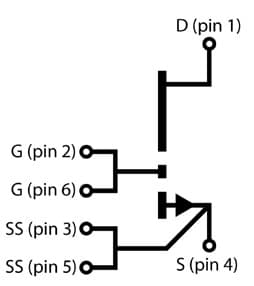
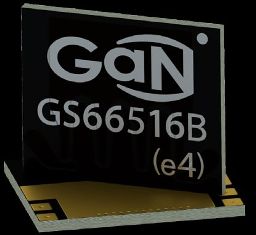
A representative GaN device is the GaN Systems GS66516B, a 650V, enhancement-mode, GaN-on-silicon power transistor that combines high current, high voltage breakdown, and high switching frequency (Figure 2). This six-contact bottom-side-cooled transistor, Figure 3, measures just 11 × 9mm and also offers very low junction-to-case thermal resistance. On-resistance is 25m?, and maximum drain-source current is 10A, while switching frequency can be as high as 10MHz and even higher. Design-in is simplified by the 0-to-6V gate-drive requirement that is enhanced by transient-tolerant gate drive of -20 to +10V.
Driver is Critical to GaN Success
It takes a properly matched and configured driver to ensure that the switching device—either GaN or MOSFET—operates to its full specifications and does not have unintended issues. In simplest terms, the role of the driver is to be the electrical interface between the lower-voltage digital output of the microprocessor-based controller or similar circuitry and the higher-voltage, high-current, slew-rate demands of the power-switching device.
Of course, there’s much more to the driver’s role than that. The driver must supply the needed current at a high enough rate to quickly charge the input capacitance at the gate of the device and to turn it on, yet without inducing ringing or overshoot; in turn-off mode, it must quickly and crisply pull that charge from the gate input, again without ringing or overshoot. It must also do so consistently, with proper skew-time control to avoid “shoot-through” short-circuits in bridge configurations.
Three factors define the top-tier concerns of driving GaN devices: The maximum allowable gate voltage, the gate threshold voltage, and the body diode voltage drop. The gate-source voltage for an enhanced GaN device is 6V, roughly half that of a MOSFET, and this simplifies the challenge of generating the needed turn-on/turn-off voltages and currents. The gate voltage is also lower than it is for most power MOSFETs and also has a lower negative temperature coefficient, which also simplifies driver-compensation issues. The forward-voltage drop of the body diode, which is an inherent part of the device structure, has a forward drop about a volt higher than comparable silicon MOSFETs.
A few numbers can make the dynamic GaN versus MOSFET situation clear. GaN can switch faster than silicon-based MOSFETs, with dV/dt slew rates in excess of 100 V/nsec. Overall GaN turn-on times are about four times faster than MOSFETs with the same RDS(ON)rating, while turn-off time is about twice as fast. While faster is better, it brings new levels of concern in the dynamic issues of the driver and associated circuitry.
There are also issues with the Miller charge that limits turn-on/turn-off speed (do you recall the Miller effect from that class on solid-state device physics?) and has an effect on waveform shape. The total Miller charge is much lower for a GaN device than it is for a MOSFET with comparable RDS(ON), so the GaN device can be turned on/off much faster, which is an advantage.
However, a high-speed dV/dt slew time can affect efficiency adversely by creating a shoot-through condition between paired devices in a bridge during the switching transition. Therefore, it is necessary to control gate-drive pull-up resistance to minimize transition time but not induce other unwanted loss mechanisms, all while also providing a way to avoid overshoot and ringing. This is needed to avoid false turn-on/turn-off glitches which are a major potential concern, as well as minimize EMI generation.
While the analysis gets fairly complicated (Figure 4 and Figure 5), the simplest solution for GaN devices where the threshold voltage is low is to split the gate pull-up and pull-down connections in the driver and allow the insertion of a discrete resistor as needed (Figure 6).
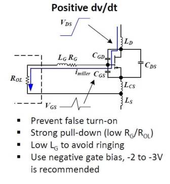
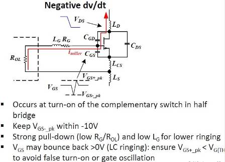
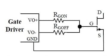
In short, a humble, passive component—the gate resistor (or resistor pair)—is a crucial element in successful drive, balancing the many related parameters. The optimum gate turn-on/off resistor ratio results in tuned performance and drive stability, so independent gate resistors for turn-on and off are recommended.
This resistor ratio is generally in range of between five and 10Ω for controlling the Miller effect. If the turn-on gate resistor is too large (typically, it is between 10 and 20Ω), the turn-on dV/dt slew rate is reduced, so switching is slowed down and losses increase. Conversely, if the slew rate is too low, there are switching losses, but this time they are due to Miller-effect turn-on as well as potential gate oscillation. For turn-off, the gate needs to be “held down” as strongly as possible with minimum impedance, so the turn-on gate resistor is typically between 1 and 2Ω for strong and fast pull-down.
Gate-driver ICs, available from many vendors, are valuable to handle many of the subtleties while still allowing the user to tailor the design specifics to the selected GaN device, the design switching speed and other factors. Among the available drivers is the LMG1205 from Texas Instruments (Figure 7), which is a gate driver for enhancement-mode GaN FETs. This IC can drive both the high-side and the low-side devices in a synchronous buck, boost, or half-bridge configuration. It has independent inputs for the high-side and low-side outputs for maximum control flexibility; peak source-current capability is 1.2A, while peak sink current is 5A to prevent unwanted turn-on during transitions. The split-gate outputs provide flexibility to independently adjust the turn-on source and turn-off sink currents.
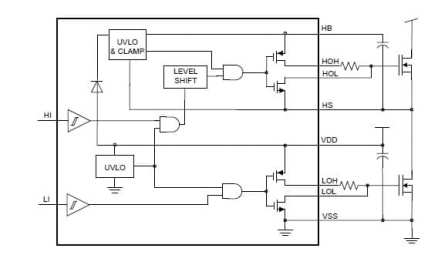
The inputs are TTL-logic compatible, yet can tolerate input voltages up to 14V regardless of the VDD rail voltage. Also, in combined high-side/low-side applications such as these, both low propagation delay and channel-to-channel skew (matching) are critical for efficiency and to avoid shoot through, so the LMG1205 features 35ns typical propagation delay and 1.5nsec propagation-delay matching.
Other available GaN drivers include the Silicon Labs Si827x series, the ADuM4223A/B family from Analog Devices, the MaximMAX5048C and the Texas Instruments LM5113. In addition, there are existing, already widely-used MOSFET drivers that have the flexibility, specifications, and features to also handle GaN devices as long as the GaN device is used at lower frequencies.
Success Takes More Than a Schematic
Every designer with any experience in high-speed circuits knows that the schematic and optimized selection of components and their values are only part of a successful and reliable system. In the case of GaN devices and circuits, it is critical to control and minimize noise coupling from power supply to the gate-drive loop. The high dV/dt and di/dt transitions, combined with low input capacitances and gate thresholds, mean that noise-induced spikes on the gate, as well as the Miller effect, may result in gate ringing or sustained oscillation. The consequences are false turn-on/off, system malfunction or even device failure.
Among their many possible causes, gate ringing and oscillation are often initiated and sustained by stray inductance in a feedback path from power supply to gate loop, as well as coupling via Miller-effect capacitance between gate and drain. Multiple, multilayered approaches are often needed to solve these problems.
The techniques include making layout changes to reduce stray inductance; minimizing external gate-to-drain coupling by locating the driver as close to the GaN device gate as possible; using low-inductance, wide PC board traces; using a Kelvin-source connection to minimize common-source inductance; and even extend to employing galvanically-isolated power supply rails. Other steps include adjusting the value of the gate-drive resistor to fine tune the turn-on slew rate; using a negative bias (-3V) for the turn off; adding ferrite beads in series with the gate to reduce high-frequency LC-ringing and overshoot; and possibly adding an RC “snubber” across the gate-source path.
Conclusion
GaN-based switching components have truly matured and now have an ecosystem of versatile devices, modeling and simulation tools, requisite drivers, applications support, field experience and more from long-established sources, less-well known vendors and even innovative start-ups. These GaN devices take power-switching into performance regions beyond what existing and even foreseeable MOSFET-based designs are able to offer. However, the speed and capabilities of these GaN devices means that even more attention and sophistication is needed to properly manage their turn-on/off characteristics with respect to gate drive, voltage and current slew rate, current levels, noise sources and coupling, layout considerations and many other factors.
Author
Bill Schweber is a contributing writer for Mouser Electronics and an electronics engineer who has written three textbooks on electronic communications systems, as well as hundreds of technical articles, opinion columns, and product features. In past roles, he worked as a technical web-site manager for multiple topic-specific sites for EE Times, as well as both the Executive Editor and Analog Editor at EDN.
 At Analog Devices, Inc. (a leading vendor of analog and mixed-signal ICs), Bill was in marketing communications (public relations); as a result, he has been on both sides of the technical PR function, presenting company products, stories, and messages to the media and also as the recipient of these.
Prior to the MarCom role at Analog, Bill was associate editor of their respected technical journal, and also worked in their product marketing and applications engineering groups. Before those roles, Bill was at Instron Corp., doing hands-on analog- and power-circuit design and systems integration for materials-testing machine controls.


