
 RECOM opens new doors with its universal half-bridge reference design which is a platform design that can be used to compare the real-life performance of various high power IGBT, 1st/2nd generation SiC, GaN, MOSFET and Cascode switching technologies. As the gate driver and PCB layout is the same for every transistor type, users will be able to compare and contrast their real-life switching performance and make informed choices about the right technology for their application.
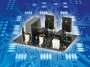
[cid:image007.jpg@01D3886D.85FF9A10]The reference design consists of a half-bridge layout with a fully isolated driver stage using isolated power supplies for both the low-side and the high-side switching transistors. Included in the package are four sets of different DC/DC converters which generate the appropriate isolated driver voltages for the different transistor types. The user can thus select which TO247 or TO247-4L (Kelvin connection) packaged switching transistors they wish to evaluate from the supplier of their choice, fit the appropriate DC/DC converter to match and then rapidly prototype and test their application. The reference design is a basic building block that can be used to evaluate forward, flyback, buck and boost topologies and by combining two or more units it can be used to evaluate full-bridge and 3-phase bridge circuits. The PCB is optimized for high-speed switching up to 1000V at up to 10A gate drive current. The signal ground is galvanically isolated from the power ground and on-board BNC sockets are fitted for high speed connections to the external TTL signal generators. As the high-side and low-side control are separate, the reference design can also be used to implement asymmetric duty cycle, active clamp and phase shifted full-bridge topologies.
 The R-REF01-HB reference design is available from all authorized RECOM distributors.
For more information please visit www.recom-power.com<http://www.recom-power.com>


 RECOM opens new doors with its universal half-bridge reference design which is a platform design that can be used to compare the real-life performance of various high power IGBT, 1st/2nd generation SiC, GaN, MOSFET and Cascode switching technologies. As the gate driver and PCB layout is the same for every transistor type, users will be able to compare and contrast their real-life switching performance and make informed choices about the right technology for their application.
 The R-REF01-HB reference design is available from all authorized RECOM distributors.


