
 As components shrink, the demand for smaller print deposits with fine pitches increases. This means that the stencils being used in a wide range of electronics manufacturing processes must be able to meet even more demanding requirements as the market moves towards finer apertures, tighter thickness tolerances, smoother surfaces, and multilevel stencils.
As a result, classic stencil manufacturing methods such as etching and laser-cutting will soon hit their limits. Alternative technologies for stencil materials and manufacturing must be sought to answer the new challenges in stencil printing.
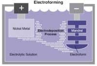
Electroforming is an advanced stencil manufacturing technology, a metal forming process whereby nickel metal is electrodeposited onto a mandrel or mould. Fundamentally, the electroforming process is similar to electroplating with the main difference being that the plated nickel is subsequently separated from the mandrel and can exist as a self-supporting structure. In the case of stencils, this will be a nickel foil with apertures which is mounted onto a frame that provides the tension required for stencil printing. ASM’s electroform business unit designs and manufactures electroformed stencils for high end printing processes for the SMT, Semiconductor and LED industries.
Key benefits:
- Better paste release as electroformed stencil apertures have a smoother side wall compared to laser cut stencils
- Reduction of solder paste bleed out with unique “cusp” or “gasket” formed around electroformed apertures
- Enable stencils with different thicknesses for different apertures on the same stencil with the Variable Aperture Height Technology (VAHT) stencils
- No need for replacement of mesh screen with dual layer stencils
For more information, please contact us at smt-solutions.sg@asmpt.com .


