Rambus Inc. recently introduced the Server Memory Interface Chipset that delivers superior performance and capacity for both the enterprise and data center server markets. The first in a family of R+ chips, the RB26 is an enhanced, JEDEC-compliant memory module chipset designed to accelerate data-intensive applications, including real-time analytics, virtualization and in-memory computing, with increased speed, reliability and power-efficiency. Data centers and enterprise markets are under increased pressure to implement enhanced memory architectures that meet the capacity and bandwidth requirements to handle large amounts of complex data. Rambus’ deep expertise in advanced memory designs makes them the newcomer to watch in the server memory chipset market.
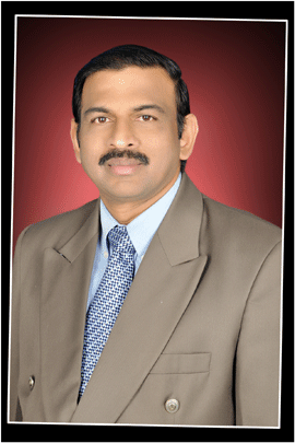
Interview with K. Krishna Moorthy, Corporate Vice President & Managing Director, India Design Center, Rambus Chip Technologies India Pvt. Ltd.
Q1. Please start with introducing your company
Rambus was founded in 1990 by two electrical engineering professionals, Drs. Mark Horowitz and Mike Farmwald. Rambus introduced a revolutionary memory architecture in the 1990s called RDRAM. Along with the revolutionary memory architecture, Rambus also pioneered an innovative business model of technology licensing. Since that time, Rambus has diversified its solutions offerings and is comprised of four main business units: Memory & Interfaces, Cryptography Research, Lighting Technology, and Emerging Solutions. Rambus recently introduced a server DIMM chipset for DDR4 systems, which is the first time in the company’s history that it is providing its own branded chips. Rambus is headquartered in Sunnyvale, CA with regional offices around the globe. Rambus has roughly 500 employees.
Q2. What are your technological core-competencies and USPs.
Rambus has core expertise in designing high-performance, low-power architectures for a wide variety of applications. Rambus has over 2,400 patents and patent applications covering a wide variety of technologies, including advancements in signal and power integrity.
Q3. Please share with us your infrastructural strengths and manufacturing set-ups
As part of our server DIMM chipset launch, we have opted for a fabless business model and partnered with a leading semiconductor foundry that has the technology and know-how to deliver the quality parts customers expect. We’ve been working in stealth mode in the past couple of years, building our product expertise and setting up an operations team dedicated to product logistics and supply chain management. In addition, we are working with key ecosystem partners in order to quickly scale and deliver high volumes. While we can’t disclose the exact manufacturing process, we are utilizing a mature, high-volume, and low-risk process from a leading semiconductor foundry.
Q4. Please tell us the growth plans of Rambus in next 5 years and targets
For the server DIMM chipset market, we believe the growth opportunity is in delivering our technology in silicon. We are entering the server DIMM chipset market with a goal of establishing ourselves as a leader and laying the foundation to provide more value-added features and functionality in the coming year. By having a blended business model, we have the opportunity to bring our technology to market where it makes the most sense, whether through licensing or delivering our technology in silicon. We are leveraging our long history in high-speed memory to address key challenges facing the industry with the goal of delivering an industry-leading product offering and roadmap. In parallel, we are taking advantage of the growth wave of big data and DDR4 in the enterprise and data center markets. We have put in place an operations and product team that will engage with a defined ecosystem and potential customers where we already have existing relationships in place.
Q5. What is your opinion is the future of Semiconductors in India.
Semiconductors in India can be split into two- Semiconductor design and Semiconductor manufacturing. The design side of it has matured over the last 10+ years very well. Starting from Verification support in late nineties to fully architected and designed semiconductor product design from India is a reality now. The engineers are able to scale up their technological competencies in tandem with the related developments in each domain and thereby mature into a level where the full design ownership now has become an accepted practice for most of the MNC captives in India. Looking into the future, this trend will continue, particularly with the present Central Government focusing their attention in Skill development. Electronics is a major vector in the National skill development initiative and this is further amplified by the push for PhD level programs being initiated and supported by the Government through Deity for Electronics including Semiconductor. These steps will have multiplier effects not only in creating high quality talent in the country but also accelerating sponsored research in top universities.
As far as manufacturing is concerned, there had been announcements about Fabs coming up but I think it is progressing at a slower pace than what was originally expected. The high capital outlay and OpEx are the reasons and the time to raise Capital to the extent of $ 5Bn at minimum is not an easy task. But in the meantime, it may be possible for the government to consider if some of the existing fabs like SCL Fab in Chandigarh etc. can be modernized and put to commercial use. Even a PPP model can be considered.
Q6. What is your opinion about “Make in India”? What are the possible obstacles & challenges?
“Make in India” is a bold and all-encompassing initiative of the present Government. As has been stated in many forums already the import bill of finished electronics goods into the country is threatening to exceed that of Oil import within the next decade which is not sustainable. So as applied to electronics sector, this is a relevant and probably a must do. The challenges are many. First and foremost is the ease of doing business in India. Tangible and visible changes need to happen in this respect. The taxation policy and its administration need to be streamlined. The mess of transfer pricing determination and administration of even simpler ones like service tax refunds etc. are a few examples to cite. The other ones are related to infrastructure which have been talked and written about in plenty already.
Q7. How closely do you work with key customers in developing new products?
Collaborating with our customers and ecosystem partners is critical. For the server DIMM chipset, we are working closely with Intel to validate our products and have their support as new contributing vendor for the Xeon ecosystem. The RB26 is currently sampling to key potential customers and critical ecosystem partners.


