
Russell Dover, general manager, Service Product Line, Lam Research Corp.

It takes a lot of different types of process tools to make chips– from deposition, to lithographic to etch and cleaning tools among others. Large scale production requires chipmakers to use fleets of the same chamber types to perform a particular processing step, such as fin etch used in making 3D transistors. Ideally, wafer lots would be processed identically across the fleet, meaning every chamber would behave exactly the same as all others. In practice, however, performance will vary from chamber to chamber due to slight differences in the many control parameters that determine the success of the process. These parameters, including pressure, temperature, power delivery and surface conditions, all have to be co-optimized.
The chamber matching challenge
The process of bringing performance closer together is called chamber matching. As chip device sizes are shrinking and process tolerances are getting more stringent, the challenges associated with chamber matching are increasing. Traditional methods have included a “golden chamber” approach or sub-component matching. The golden chamber method involves defining one chamber as ideal and attempting to tune all others to produce the same results. Sub-component matching focuses on the hardware subsystems and defines rigorous tolerance specifications that each chamber has to satisfy. The assumption of this approach is that if all components of each chamber match identically, then the chamber as a whole should match. Both of these traditional methods have limitations when it comes to complex physical and chemical interactions of advanced plasma processing. Matching chamber performance requires smart tools and services.
A proven solution
Lam Research’s approach to creating smart tools is to make them self-aware, adaptive, and self-maintaining. The Equipment Intelligence® Data Analyzer from Lam has been used broadly for fleet matching and big data analytics of etch chambers on its2300® platform. Many fabs around the world have widely reported dramatic improvements in chamber matching performance, more rapid troubleshooting of chamber issues, improvements to uptime and improvements in mean time between cleans (MTBC).
The approach taken is to look at large data sets of tool sensor output from wafer processing and to identify the natural distribution within a fleet of chambers to detect mismatched chambers, then to drill down to a root cause and correction. This method is a big data multivariate machine learning approach, which looks at many signals within a chamber or within a chamber subsystem. When combined with customer fab information, this can reduce chamber matching times from weeks to days.
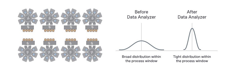
An illustration of a fleet of Lam 2300® etch systems (each with six separate chambers) and their process distribution before and after Lam’s Equipment Intelligence® Data Analyzer big data machine learning analysis
The latest version of the Equipment Intelligence® Data Analyzer was designed for plasma-enhanced chemical vapor deposition (PECVD) and atomic layer deposition (ALD) chambers. It accommodates differences in the wafer flow scenarios in PECVD/ALD chambers in relation to etch chambers (multi-pedestal vs. single wafer chambers). Parsing schemes enable individual wafer movement to be tracked across multiple-station process modules. The software includes accommodations to deal with recipe blocks, sub-recipes and multiple recipe iterations, all unique characteristics of PECVD/ALD wafer flows.
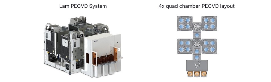
Different views of a Lam PECVD process tool with four quad station (four wafers at a time) chambers
Virtual sensor innovation
This smart tool approach is being utilized at high volume manufacturing (HVM) customer sites and is accelerating critical customer requirements, such as extending preventive maintenance cycles and improving uptime. This includes the creation and deployment of predictive control charts based on regression models, the use of classification models for predicting metrics and notifications sent to key personnel to allow for early warnings and rapid resolution of potential problems. The use of virtual metrology-based regression models allows for the prediction of production performance as well as an easy drill down to the root cause of production trending. Lam’s Data Analyzer has also been used in a reactive fashion to quickly diagnose multiple critical tool issues such as chamber matching or unscheduled down time.
One of the key objectives of using these big data machine learning approaches in HVM semiconductor manufacturing is to allow process tools to achieve higher productivity (more good wafers out at lower cost) than ever before.
Conclusion
Data is the backbone for smart tools and services that address the chamber matching challenge. The Equipment Intelligence® Data Analyzer creates a repository of Lam equipment data within its customer facilities. Data integrity is maintained, and customers have the ability to control and access the data. This flexible backbone enables solutions that meet the challenge of maintaining complex systems in a HVM environment, as well as the tight process tolerances needed for device yield. Learn more at https://www.lamresearch.com/.


