Contributed By Digi-Key’s North American Editors
2019-05-15
Automakers are increasingly developing electric vehicles (EVs), but their short driving range remains problematic. While aerodynamic design, lighter materials, and more efficient power usage do help, it’s not enough. Automotive power electronics designers need to use advanced wide bandgap semiconductor (WBG) materials to meet efficiency and power density requirements.
Comprising primarily gallium nitride (GaN) and silicon carbide (SiC), these materials are an improvement over incumbent semiconductor technologies like silicon (Si) metal-oxide semiconductor field-effect transistors (MOSFETs) and insulated-gate bipolar transistors (IGBTs) by offering lower losses, higher switching frequencies, higher operating temperature, robustness in harsh environments, and high breakdown voltages. They are particularly useful as the industry moves toward higher capacity batteries that operate at high voltages with shorter charging times and overall reduced losses.
This article will provide a brief overview of WBG technology and its role in automotive EV electronics. It will then introduce suitable GaN and SiC solutions, from ROHM Semiconductor, STMicroelectronics, Transphorm, and Infineon Technologies, and Infineon Technologies, and provide guidance on their application.
The advantages of WBG semiconductors
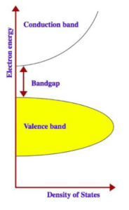
By way of review, a bandgap is the energy needed to excite electrons from a material’s valence band into the conduction band, and WBG materials have bandgaps significantly greater than that of silicon (Figure 1). While Si has a bandgap of 1.1 electron volts (eV); SiC has a bandgap of 3.3 eV, and GaN has a bandgap of 3.4 eV.
WBG semiconductors permit devices to operate at much higher voltages, frequencies, and temperatures than conventional silicon. What’s more, switching and conduction losses are lower. WBG materials have roughly ten times better conduction and switching properties than Si. These abilities make WBG technology a natural fit for power electronics, particularly for use in EVs, as SiC and GaN components can be made smaller, can operate faster, and are more efficient.
The benefits of WBG devices must be balanced against manufacturing complexity and higher cost to mass produce. While WBG components may be initially more expensive their cost continues to fall, and generally speaking they will realize overall system cost savings. For example, the use of SiC devices in an EV might add an additional upfront cost of several hundred dollars, but result in an overall cost savings from lower battery costs, reduced space requirements, and simpler cooling measures such as smaller heatsinks or convection cooling.
SiC for the main inverter
The traction inverter, which controls the traction electric motor in EVs, is an example of a key EV system that can benefit from WBG components. The inverter’s core function is to convert a DC voltage to a three-phase AC waveform to drive the EV’s motor, and then convert the AC voltage developed by regenerative braking back to a DC voltage to recharge the battery. Since the inverter converts energy stored in the battery pack to AC to drive the electric motor, the lower the losses in that energy conversion, the more efficient the system. The enhanced conductivity and faster switching frequency of SiC devices, as compared to silicon, reduce power loss because less energy is lost as heat. Ultimately, the higher efficiency of SiC-based inverters will show up as higher EV mileage.
Power modules that handle large currents are typically IGBT types that combine Si IGBTs with Si fast recovery diodes (FRDs), a configuration commonly used in automotive inverter modules. However, SiC provides higher operating temperature and higher switching speeds than the Si IGBT incumbents. These capabilities are optimal for traction inverters given their critical need to transfer large packets of energy to and from the battery.
Here’s why: as the IGBT is a switching element, its switching speed (turn-on time, turn-off time) is one of the key parameters influencing efficiency (loss). With IGBTs, low resistance at high breakdown voltage is achieved at the cost of switching performance; during device turn-off there is “dissipation time,” which increases switching loss. As a result, IGBTs have relatively low efficiency. If MOSFETs are used instead of IGBTs in inverter modules, it is possible to achieve higher efficiency because of their shorter turn-off time and higher operating frequency. Yet Si MOSFETs also present problems; they have a large “on” resistance compared to Si IGBTs.
Taking advantage of SiC’s favorable characteristics, SiC MOSFETs, which are almost half the size in die area compared to IGBTs, can combine four desirable characteristics of a power switch:
- High voltage
- Low on resistance
- Fast switching speed
- Low switching losses (especially turn off losses)
The wider bandgap also means SiC devices can normally operate at temperatures ranging from 150°C to 175°C, and when properly packaged, 200°C or higher.
As SiC Schottky barrier diodes (SBDs) are concerned, in a SiC SBD a metal junction with the SiC semiconductor is formed to obtain a Schottky barrier. But unlike silicon FRDs, their advantages do not change significantly over wide current and operating temperature ranges. A SiC part also has a dielectric breakdown field some ten times higher than that of silicon. As such, SiC products with a rating of 1200 volts are now being mass produced, so costs are falling accordingly. Additionally, products rated at 1700 volts are under development.
SiC diodes also do not show forward and reverse recovery losses, just a small amount of capacity charge losses. Studies have shown the switching losses can be 90% less with SiC SBDs over Si fast recovery diodes, where the junction temperature affects recovery current and recovery time. As a result, SiC diodes yield a considerably lower figure of merit (FoM) (Qc x Vf) compared with Si diodes. Lower FOM implies lower power losses and therefore better electrical performance.
There are some drawbacks with silicon carbide material. One of which is a positive thermal coefficient, meaning the higher the temperature the higher the forward voltage (Vf). If the current through the diode increases the forward voltage drop also increases. This conduction loss can lead to thermal runaway when higher currents are applied to the diode.
Taken together, however, SiC MOSFETS and SBDs allow system designers to improve efficiency, lower the size and cost of the heatsink, increase the switching frequency to reduce the size of the magnetics, and shrink the cost, size and weight of the final design. An EV inverter using SiCs can be made 5x smaller, 3x lighter, and have 50% lower power loss than an Si-based equivalent.
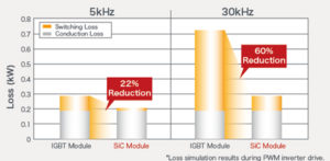
For example, ROHM Semiconductor developed the BSM300D12P2E001 half-bridge SiC power modules that integrate SiC MOSFETs with SiC SBDs into a single package, minimizing the switching loss previously caused by IGBT tail current and FRD recovery loss (Figure 2).
ROHM Semiconductor’s SiC-based MOSFETs have a stated loss reduction of 73% when compared to IGBTs. Their range of MOSFETs can handle up to 1700 volts with an on resistance ranging from 45 milliohms (mΩ) to 1150 mΩ. They come in TO-247N, TO-3PFM, TO-268-L, and TO-220 packages.
ROHM also produces AEC-Q101 automotive-qualified SiC Schottky barrier diodes which have short recovery times, high-speed switching capabilities, low temperature dependence, a low forward voltage, and the ability to handle up to 650 volts at currents between 6 and 20 amperes (A).
The role of SiC devices in EVs
Tesla was the first electric car manufacturer to integrate a full SiC power module for its main inverter, doing so in the Tesla Model 3 sedan. Tesla’s previous cars, the model S and model X, used IGBTs in TO-247 packages. Collaborating with STMicroelectronics, the Tesla inverter is composed of SiC power modules assembled on a heatsink.1 The MOSFETS, like STMicroelectronics’ SCT10N120, are rated at 650 volts and are thermally dissipated using copper baseplates.
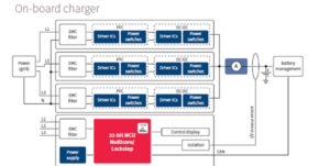
The charging device for EVs comes factory installed and is called the “on-board charger” (OBC). In an EV or plug-in hybrid EV (PHEV), the OBC provides the means to recharge the battery from the AC mains either at home or from outlets found in private or public charging stations. The OBC uses AC/DC converters to convert 50/60 Hertz (Hz) AC voltage (100 to 240 volts) to a DC voltage to charge the high-voltage traction battery (usually around 400 volts DC). It also adjusts the DC levels to the battery requirements, provides galvanic isolation, and includes AC/DC power factor correction (PFC) (Figure 3).
GaN gaining traction for efficiency
A design requirement for OBCs is to have the highest possible efficiency and reliability to ensure rapid charging times while meeting the limited space and weight requirements of the EV manufacturer. OBC designs using GaN technology can simplify EV cooling systems and reduce charging time and power losses. Commercial GaN power devices are lagging somewhat behind SiC in terms of automotive market share, but they are demonstrating impressive performance and are gaining traction very quickly. Like SiC devices, GaN devices offer lower switching loss, faster switching speeds, increased power density, and enable overall system size, weight, and cost reductions.
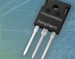
For example, Transphorm’s TP65H035WSQA is an automotive grade AEC-Q101-qualified GaN FET that performed up to 175°C during qualification testing (Figure 4). The device has a typical on resistance of 35 mΩ in a standard TO-247 package. As with its predecessor, the 49 mΩ Gen IITPH3205WSBQA, the device targets AC/DC OBCs, DC/DC converters, and DC/AC inverter systems for plug-in hybrid electric vehicles and battery EVs, for which It enables AC/DC bridgeless totem-pole PFC designs.
While a typical Si MOSFET has a maximum dV/dt rating of 50 volts/nanosecond (ns), the TP65H035WS GaN FET will switch at dV/dt of 100 volts/ns or higher to achieve the lowest possible switching loss. At this level of operation, even the layout becomes a significant contributor to performance. The recommended layout keeps a minimum gate drive loop and keeps the traces between the switching nodes very short, with the shortest practical return trace to the power bus and ground. The power ground plane provides a large cross-sectional area to achieve an even ground potential throughout the circuit. The layout carefully separates the power ground and the IC (small signal) ground, only joining them at the source pin of the FET to avoid any possible ground loop
Also developed for OBC applications in hybrid and electric vehicles, Infineon’s AIDW20S65C5XKSA1, part of the company’s fifth-generation CoolSiC automotive Schottky diodes, complements the company’s IGBT and CoolMOS portfolio and meets automotive application requirements in the 650 volt class.
Thanks to a new passivation layer concept, this is one of the most robust automotive devices available in the market with regard to humidity and corrosion resistance. Because it is based on a 110 micrometer (µm) thin wafer technology, it also demonstrates one of the best FOMs in its category, implying lower power losses and therefore better electrical performance.
Compared to the traditional Si FRD, the Infineon CoolSiC Automotive Schottky Diode improves the efficiency of an OBC by one percentage point over all load conditions.
Using SiC and GaN devices
Along with careful layout, mentioned earlier, one potential issue with SiC parts is their driving requirements, which are very different than IGBT devices. While most transistors typically have driving requirements that use symmetric rails (such as ±5 volts), SiC devices require a small negative voltage to ensure that they are fully off, and so they require rails that are asymmetric (e.g. -1 volt to -20 volts).
Further, while SiC has superior thermal properties and is capable of conducting large amounts of thermal energy compared to silicon, SiC parts may be housed using packaging designed and employed for Si, such as die bonding and wire bonding. While this method for packaging may work well with SiC, it is only practical for lower frequency circuits (tens of kHz). As soon as high frequencies are used, parasitic capacitance and inductance become too great, preventing a SiC-based device from realizing its full potential.
Similarly, to use GaN devices at their full potential, packaging must have both very low parasitic inductance and high thermal performance. New packaging approaches such as embedding dies in packages similar to a multi-layer pc board have achieved the required performance at low cost, while also eliminating wire bonds which bring their own device reliability concerns.
A key element that acts as an interface between the controller and power device is the gate driver. Gate drive design is always a concern for electronics designers adopting new devices and it is important to understand how to drive SiC and GaN power devices. Requirements are:
- A high supply voltage to realize high efficiency through low conduction losses
- A high drive strength to realize low switching losses
- Fast short-circuit protection
- Smaller propagation delay and variation, for high efficiency and fast system control
- High dv/dt immunity
Some early GaN devices required special drivers to prevent gate overvoltage conditions. New generation E-HEMTs with wide Vg tolerance are now available and can be driven by many standard MOSFET drivers simply by changing the gate voltage supply. GaN FETs are lateral devices and thus require a relatively low optimal drive voltage. So, in total, GaN devices have similar gate drive requirements to Si MOSFETs and IGBTs. Requirements include:
- Smaller gate charge – lower drive loss, faster rise and fall time
- Lower gate voltage
- Negative voltage to improve gate drive robustness
- Slew rate control using a gate resistor
The upside is that many providers of SiC and GaN solutions are including the additional electronics inside the package so they can be drop-in replacements for current designs.
Conclusion
To meet the efficiency and power density requirements of EV systems such as inverters and on-board chargers, automotive power electronics designers are now able to take advantage of more advanced WBG semiconductors such as SiC and GaN. These offer lower losses, higher switching frequencies, higher operating temperature, robustness in harsh environments, and high breakdown voltages compared to traditional silicon devices.
GaN and SiC can operate at higher temperatures with a similar expected lifetime or can operate at similar temperatures as Si devices with a longer life. This provides the design engineer with different design paths depending on the application requirements.
Use of WBG materials also allow designers to choose from multiple strategies to fit their design goals: use the same switching frequency and increase the output power; use the same switching frequency and decrease the amount of heat sinking required by the system, saving on total cost; or increase the switching frequency while maintaining the same power losses in the switch.


