
CoolMOSTM CE is Infineon’s high-voltage power MOSFET designed for consumer electronics and lighting products. Engineered on Infineon’s super junction technology platform, the CoolMOSTM CE series delivers excellent performance. As the product is cost optimized, its cost performance ensures that it remains highly competitive in such extremely price-sensitive markets as consumer and lighting applications. This article proves the products excellent performance through charger case.
Advances in modern technology have brought about a boom of consumer electronics, represented by the popularity of smart phones, tablet PCs, e-readers, LCD / LED TVs and laptops as well as the ascendance of new products and new connectivity concepts such as wearable devices, Internet of Things and smart home. Meanwhile, advances in power electronic and semiconductor technologies have made LED lamp, a new lighting product, accessible to consumers. Featuring high energy efficiency, high light conversion efficiency, long life time, and rich colours, LED lamps which are more environmentally friendly, have gradually replaced traditional light sources like tungsten and fluorescent lamps.
Infineon’s product solutions
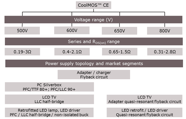
Figure 1 shows the overview of CoolMOSTM CE. Offering 500V, 600V, 650V and 800V devices, CoolMOSTM CE is one of the CoolMOSTM portfolios with the widest voltage range. The CoolMOSTM CE series is designed in a DC in-resistance range of 0.19Ω ~ 3Ω to meet needs of different power levels and application scenarios
Its application fields include consumer electronics and lighting products such as adapter / charger, computer / server power supply, TV power supply and LED lamp driver.It is applicable to many power conversion topologies including hard switching topologies such as hard-switch flyback, quasi-resonant flyback, PFC circuit, two-transistor forward, as well as soft switching topologies such as LLC.
This brings power conversion device designers great convenience, enabling them to just limit one power switch while selecting different circuit schemes based on design requirements.
CoolMOSTM CE is designed on Infineon’s superjunction technology platform, while most of the power MOSFET devices for consumer electronics and lighting products currently available in the market are based on the standard MOSFET technology. Compared to the standard technology, the superjunction technology has obvious advantages in multiple key parameters.
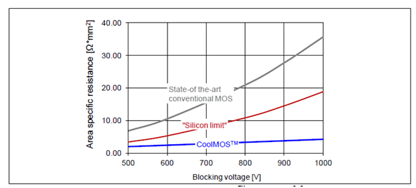
- Lower RDS(on) (drain-source on-resistance) and lower conduction loss. Figure 2 shows a comparison of product of drain-source on-resistance and chip area (RDS(on) × A) between the conventional standard MOS and the CoolMOSTM product at different drain-source block voltage levels (equivalent to drain-source on-resistance in the case of the same chip area) and gives the “silicon limit” curve of the conventional technology. As can be seen from the figure, for the MOS adopting the conventional standard technology, its drain-source on-resistance increasing with its blocking voltage and cannot be smaller than the theoretic “silicon limit”. For the CoolMOSTM product adopting the superjunction technology, the product of its drain-source on-resistance and its chip area is much lower than that of the conventional standard MOS and the “silicon limit” and virtually does not increase with its blocking voltage. So, the CoolMOSTM product’s DC on-resistance is smaller in the case of the same chip area and its chip area is smaller and cost lower in the case of the same DC on-resistance.
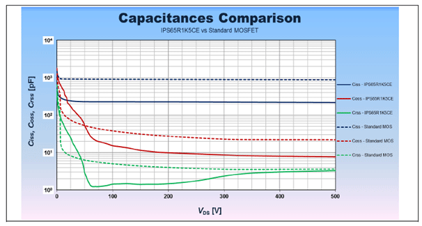
- Lower parasitic capacitances (Ciss, Crss, Coss), better switching features and lower loss. Figure 3 shows a comparison of parasitic capacitances between CoolMOSTM CE (IPS65R1K5CE) and the standard MOSFET with a similar drain-source on-resistance. In the figure, the solid lines represent CoolMOSTM CE and dotted lines the standard MOSFET. As can be seen from the figure, for CoolMOSTM CE, its three parasitic capacitances – Ciss (equivalent input capacitance), Crss (equivalent transfer capacitance / Miller capacitance) and Coss (equivalent output capacitance) – are all smaller than the counterparts of the standard MOSFET. CoolMOSTM CE has smaller parasitic capacitances because it adopts the superjunction technology. As shown in Figure 2, in the case of similar drain-source on-resistances, the product adopting the superjunction technology features smaller chip size and in turn smaller parasitic capacitances. Smaller Ciss and Coss ensure lower driving and switching losses. Smaller Crss makes CoolMOSTM CE’s gate oscillation smaller, reliability higher and EMI better.
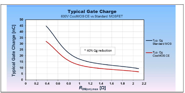
- Smaller gate charge, lower driving loss and faster switching. Figure 4 provides a comparison of gate charge vs. drain-source on-resistance between CoolMOSTM CE and the standard MOSFET. As can be seen from the figure, CoolMOSTM CE’s gate charges are averagely about 40% lower than the counterparts of the standard MOSFET at different drain-source on-resistances. Smaller gate charge means driving loss is smaller at the same driving voltage and frequency and faster switching at the same driving current, which ensure lower loss and higher efficiency.
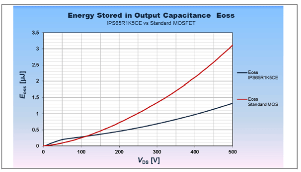
- Lower energy stored in output capacitance and lower loss. Figure 5 compares the energy stored in output capacitance (Eoss) between CoolMOSTM CE (IPS65R1K5CE) and the standard MOSFET. As shown, in the case of a higher drain-source voltage (> 120V) (for a high-voltage MOSFET, its drain-source voltage is definitely not lower than 120V; otherwise the selection of the high-voltage MOSFET is meaningless), CoolMOSTM CE’s energy stored in output capacitance is lower than that of the standard MOSFET. Since the energy stored in output capacitance loses into the MOSFET in the form of heat after the MOSFET is on, lower energy stored in output capacitance means lower MOSFET loss and higher efficiency.
As can be seen from these parameter comparisons, CoolMOSTMCE delivers obvious advantages in efficiency and reliability compared to the standard MOSFET. Next, CoolMOSTMCE’s superior performance will be verified through charger and LED driver cases.
Charger Case
This case involves a 15W charger in the global input range, with main specifications as follows:
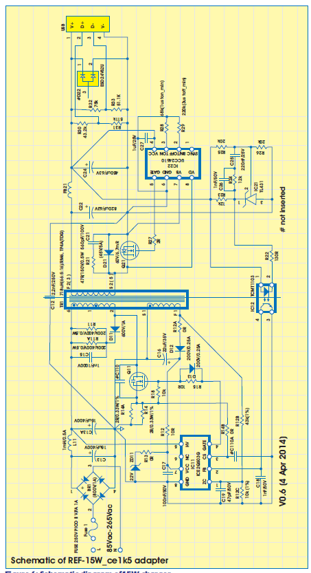
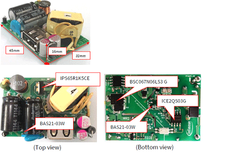
Figure 6 shows a detailed schematic diagram of the charger. The charger adopts the flyback synchronous rectification scheme. Its primary side control IC is Infineon’s quasi-resonant PMW current mode control IC ICE2QS03G[1], primary side main power switch Infineon’s CoolMOSTMCE 650V voltage-proof MOSFET IPS65R1K5CE[2], secondary side synchronous rectification control drive IC TI’s UCC24610 and synchronous rectification MOSFET Infineon’s BSC067N06LS3 G[3] from the OptiMOSTM (Infineon’s medium- and low-voltage (20V ~ 250V) power MOSFET brand) series. The charger provides complete start-up and protection features, including soft start, operation in burst mode at light load, auxiliary power supply over-voltage protection, output overload / open loop protection, over temperature protection and automatic recovery, adjustable output overvoltage protection and secondary side winding short circuit protection.
The charger has been tested thoroughly, with results as follows:
- Efficiency test. According to the results shown in Figure 8, the average efficiency is 89.05% at 115Vac input and 88.24% at 230Vac input, which meet the specifications in Table 1. According to the results shown in Figure 9, the 10%-load efficiency is 87.05% at 115Vac input and 85.08% at 230Vac input, also complying with the specifications.
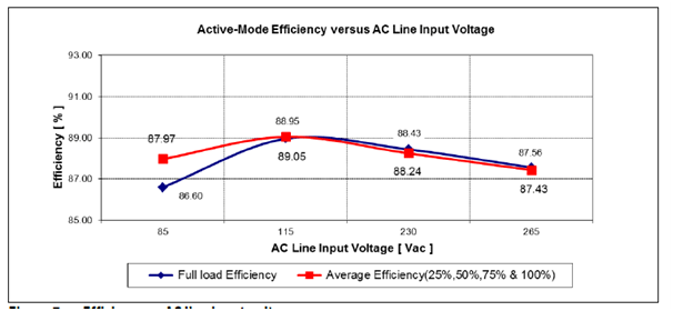
Figure 8: Average efficiency and full load efficiency vs. input voltage 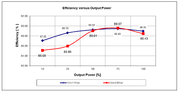
Figure 9: Efficiency vs. load at different input voltages - No-load loss. Figure 10 shows the standby power consumption (no-load loss) vs. input voltage. No-load loss is smaller than 40mW across the whole input voltage range, which meets the specifications.
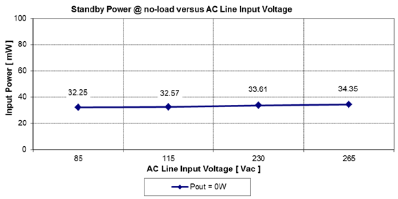
Figure 10: No-load loss vs. input voltage - Conducted noise test. Figures 11 and 12 respectively show the conducted noise test results of the input live and neutral wires at 115Vac and 230Vac inputs and full load output. The conducted noises comply with EN55022 (CISPR22) Class B, with more than 8dB margin in terms of quasi-peak noise.
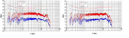
Figure 11 Conducted noises of live and neutral wires at 115Vac input and full load output 
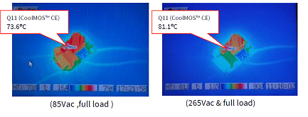
- Temperature test. Figure 13 shows the temperature test results of power MOSFET IPS65R1K5CE at 85Vac and 265Vac inputs and full load output. Its case temperature is lower than 90°C at the minimum and maximum input voltages.


As can be seen from the above results, the charger adopting Infineon’s CoolMOSTM CE and integrated solution delivers excellent performance and high cost performance enabled with the excellent cost competitiveness of CoolMOSTM CE.
Conclusion
This article proves CoolMOSTM CE’s applicability to consumer electronics through the charger. For CoolMOSTM CE, the superjunction technology enables excellent performance whilst positioning for consumer electronics ensures high cost competitiveness. In conclusion, Infineon’s CoolMOSTM CE is the highest-performance semiconductor solution for consumer electronics and lighting applications.
About the author
Owen Song: Currently Song is working for Infineon China as an application engineer at the director level engaged in research on application of Infineon products in the field of switching power supplies. He once worked for Emerson Network Power and Huawei Technologies Co., Ltd., where he was engaged in R&D of primary and secondary power supply products for communications applications. Song holds a master’s degree from the Department of Electrical Engineering, Harbin Institute of Technology.


