By Michael D. Capili, Sr. Process Engineer, STMicroelectronics
MEMS stands for Micro Electromechanical Systems, which is a technology that in its most general form can be defined as miniaturized mechanical and electro-mechanical devices and structures that are made using the techniques of microfabrication. MEMS, as shown in Figs 1 and 2, are ultra-compact systems composed of micro-mechanical components such as sensors, actuators, and electronic circuits on a silicon wafer using the microfabrication technology of the manufacturing technology. Typically, the architecture of a MEMS package is composed of 2 kinds of silicon die: (1) MEMS die which is fabricated with the microscopic moving parts, and (2) the ASIC die that contains the functional circuit for the MEMS. The critical physical dimensions of MEMS devices can vary from well below one micron on the lower end of the dimensional spectrum, all the way to several millimeters. Likewise, the types of MEMS devices can vary from relatively simple structures having no moving elements, to extremely complex electromechanical systems with multiple moving elements under the control of integrated microelectronics. Due to the complexity of the package need to upgrade the current Die attach machine to meet the product requirement.

Experimental Details
Due to product structure criticalities most of MEMS products, are processed using the latest Die Attach machine model, with the capability of 30mm accuracy of Die Placement, can process Wafer with double Die Orientation 0° and 180° bonding and can detect for a wrong die Orientation and lastly can process thin substrate 130mm.


The old Die Attach machine model such as ASM383 die attach machine is not capable to process with Die Orientation 0°and 180° bonding, that can lead to wrong die orientation issue. Machine also need improve the detection for wrong die Orientation. Also, the machine work holder needs to enhance to process thin substrate (130m) to prevent the Damage Substrate problem.
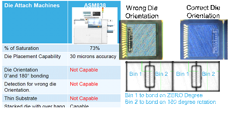
In order to meet the MEMS product requirement in Die Attach, need to upgrade and enhance the old model Die Attach machine capability, below the machine activities to overcome the criticalities of MEMS refer to Table 1.
| Criticality | Potential defect | Action |
| Wafer die orientation 0°and 180° bonding | Wrong Die Orientation Shifted Map | Performed machine bond head overhaul by replacing major parts & perform calibration upon re installation.Installation of new BHT bond arm. Replacement of 24-00520 BH Y LMGUIDE 2SRS12MSSC1+220LP Replacement of 24-00519 BHZ LMGUIDE 2SRS9MUUC1E+95LPM11Replacement 12-E60686 AD838 BHT M&ENC& BF flex cableReplacement of 02-75527 BA BF 3W-VCM coil with thermalSoftware upgrade – CSW V 9.28.53 / VSW 3.56.47 |
| Thin substrate 130mm | Damaged/ crumpled leadframe | Upgrade the workholder – Installed roller at Workholder to compensate the substrate warpage. |
| Die placement < 30 microns | Misplaced die | Bond head & optics calibration.Bond arm planarity3 pt. alignmentOptics calibrationBond optics glass calibrationBond head theta calibrationLVDT calibrationPerformed device set upTeach LF indexingTeach bond, Post bond & wafer, wafer alignment pt. PRLearn pick & bond level |
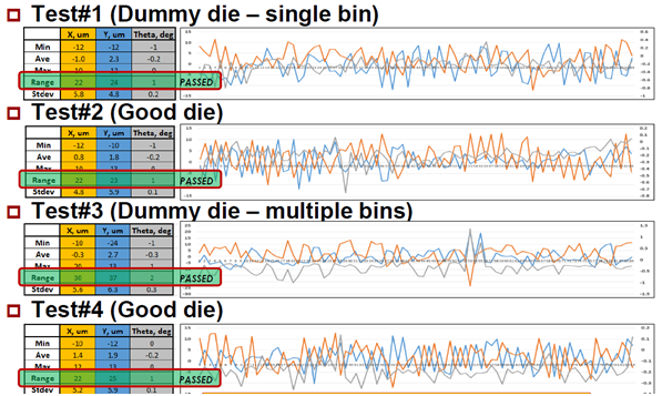
After the mechanical and software upgrade a machine test was performed to check the machine accuracy in terms of die placement. A different test scenario was done and measure the actual die placement X and Y axis and the die theta or orientation.
Results And Discussion
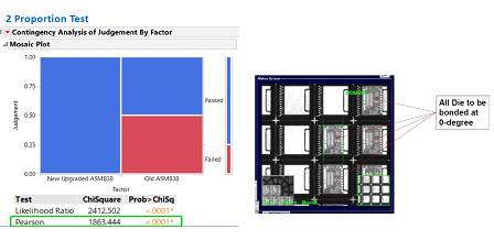
After the completion of machine upgrade and enhancement, a Statistical Validation using 2 Proportion tests, was performed to check the effectivity of the actions. First Statistical validation does the upgraded or new version of ASM838 is capable to bond the wafer with Die Orientation 0°and 180° bonding. The statistical result is shown at a 95% confidence level. there is a Significant difference the New upgraded ASM838 is capable to process wafers with Die Orientation 0°and 180° bonding.
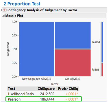
The second Statistical validation does the upgraded or new version of ASM838 is capable to detect the Wrong Die Orientation at Post Bond Inspection. The statistical result is shown at a 95% confidence level, there is a Significant difference the New upgraded ASM838 is capable to detect Wrong Die Orientation during post bond inspection.
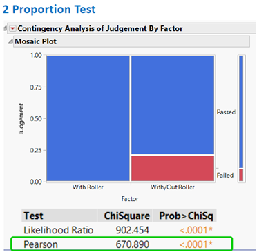
Lastly, the third Statistical Validation, does the installation of an additional roller in the work holder will reduce the occurrence of Damaged substrate. The statistical result is shown at a 95% confidence level, there is NO Significant difference the New installed roller in ASM838 can reduce occurrences of Damaged Substrate.
Conclusion
The overall practical conclusion is the new upgraded and enhancement on ASM838 die attach machine is capable to process MEMS package, can overcome the product structure criticalities such us 30um accuracy for Die Placement, can process Wafer with double Die Orientation 0°and 180° bonding and can detect for wrong die Orientation, and lastly can process Thin Substrate130um. The new upgraded machine has the same capability, and performance of the new die attach machine model, therefore the upgrade and enhance the old model Die Attach machine is effective and successful.
References
- Die Attach Manual by ASM Pacific Technology www.asmpacific.com
- JMP Design of Experiments, Release 14 Copyright © 2019, SAS Institute Inc., Cary, NC, USA ISBN 978-1-59994-413-5.
- John H. Lau, Chengkuo Lee, C. S. Premachandran and Yu Aibin. Advance MEMS Packaging, The McGraw-Hill Companies, Inc. 2010, pp 26 -30.
- V. Thiyagarajan. Micro Electromechanical Systems (MEMS) from Lakshmi Publications Anna University 2013
- Nadim Maluf and Kirt Williams. An Introduction to Microelectromechanical Systems Engineering, Second Edition by
- Jan Korvink; Oliver Paul; Jan Korvink. Mems: A Practical Guide to Design, Analysis and Applications, December 2006
- Markku TilliMerviPaulasto-Kröckel Matthias Petzold Horst TheussTeruakiMotookaVeikkoLindroos. Handbook of Silicon Based MEMS Materials and Technologies 3rd Edition Editors: by Elsevier Published Date, 17th April 2020.
- Jan G. Korvink and Oliver Paul. MEMS A Practical Guide to Design, Analysis, and Applications Book • 2006.
- Yole Development. Status of Advanced Substrates 2019 report by Published on May 17, 2019
- Tai-Ran Hsu. Mems Packaging (EMIS Processing) (Materials, Circuits and Devices) Dec 1, 2003


