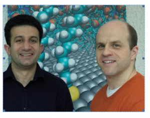
Virtual insight into atomic-level ALD offers large-scale opportunity for semiconductor industry

Researchers at Tyndall National Institute, Ireland, have produced the first ever atom-by-atom simulation of nanoscale film growth by atomic layer deposition (ALD) – a thin-film technology used in the production of silicon chips.
Present in all electronic devices such as credit cards, mobile phones and computers, each chip is made up of multiple thin layers that provide different functions. ALD has a key role to play in the manufacture of chips with ever thinner layers for the next generation of electronic devices. Growth simulations could help to improve the ALD process, but until now, were not accurate enough over experimental timescales.
Similarly, while quantum mechanical simulations give an accurate atom-by-atom picture of individual ALD reactions at the tiniest scales, this is still far removed from what can be measured in the lab – until now. The Tyndall group led by Dr Simon Elliott has for the first time combined the accuracy from the quantum mechanical level with the statistics needed to follow how thousands of atoms react millions of times a second, building up layers of material, as in the lab.
Mahdi Shirazi, who will be awarded a PhD for this work, explains what set his research apart: “It was crucial to model the complete set of all ALD reactions; hundreds of them, at the quantum mechanical level and then carefully extract the information that was needed for the growth simulations.”
Thus, for the first time, we see the link between atom-by-atom chemical reactions and the growth of layers of materials. This opens the way to new and improved ALD processing of materials for electronic chips, but also for catalysts, solar cells and LED lighting.
The simulations were made possible through the computational power of the Irish Centre for High End Computing and the project was funded by Science Foundation Ireland through the FORME strategic research cluster.


