 One of the most common measuring tasks in RF engineering is the analysis of circuits, from simple filters and amplifiers to complex satellite communication modules.
Nowadays, semiconductor technology requires that integrated circuits be interconnected at very high-speed data rates. Taking time domain measurements on the digital links can offer challenges for electronic engineers, one of which is to decide which is the better measurement instrument to use in the given signal integrity environment.
Signal-integrity design considerations must be considered upfront to ensure the robust operation of modern high-speed digital systems.
As an extremely versatile test instrument, a VNA is the ideal equipment for quickly and precisely uncovering signal integrity problems, such as reflections and crosstalk.
Multigigabit/s connections between chips that are linear and time-invariant can be completely characterized by measured parameters – called network parameters — at their terminals irrespective of their internal configuration. Moreover the measured parameters of any such individual component, such as connectors and PCB traces, can be used to determine the network parameters of any configuration containing these components.
S-parameters are being used more and more in high speed digital design because (as microwave engineers have known for decades) they are easier to measure and work with than other kinds of parametric models. Although s-parameters are a frequency-domain representation, they can be combined easily with time-domain techniques such as SPICE and IBIS IC models, and eye pattern diagrams by use of convolution (IFFT) methods.
Overcoming Embedding/de-embedding Challenges Associated with Today’s High-frequency Component Designs (Courtesy: Anritsu)
Traditional de-embedding techniques are oftentimes insufficient for today’s high-speed component designs utilized in high data rate applications. As frequencies approach 70 GHz or even 110 GHz, errors associated with fixturing can mask the behavior of the device under test (DUT). Poor de-embedding can lead to both passivity and causality errors. In addition, high fixture loss may affect the accuracy and repeatability of de-embedding.
Signal integrity engineers given the task of overcoming these challenges have found that a new generation of Vector Network Analyzers (VNAs) can help them gain greater confidence in their designs. Some modern VNAs, such as the Anritsu VectorStar™ MS4640B utilize a unique instrument architecture, as well as special software tools to help make embedding/de-embedding straightforward and simple.
New de-embedding capabilities offered in VNAs can be used to remove test fixture contributions, modeled networks and other networks described by S-parameters (S2P files) from the measurement results for greater accuracy and repeatability. Similarly, enhanced embedding functionality can simulate matching circuits to optimize DUT performance, which is helpful in amplifier design applications. The function can also be used to add effects of a known structure to a measurement. With the new capabilities, engineers have a greater ability to locate design weaknesses, such as discontinuities, impedance changes, and crosstalk issues in high-speed DUTs.
Let’s continue to use VectorStar as an example. With the VNA, engineers can combine a wide range of calibration capabilities with up to seven de-embedding techniques to address the various situations found in many high-frequency component designs. By matching the calibration and de-embedding method to specific DUT and fixture structures, measurement accuracy and repeatability are improved. In addition, external software is no longer necessary to de-embed differential devices, for faster and more accurate differential device analysis.

Mr. Madhukar Tripathi, Anritsu India Pvt. Ltd. highlights some key points about VNA market, technology performance and latest VNA range.
“VNA Market is growing in India. VNA are used in educational and research institute. Telecom products are also tested using VNA. VNA plays an important role in final testing of many electronics consumer products.
Anritsu have introduced NLTL- Non Linear Transmission Line technology based VNA. This is patented technology. NLTL based VNA provides better cost performance ratio to users.
Anritsu offers a variety of vector network analyzers (VNAs) to suit your application. Choose from an RF VNA to a Broadband VNA, from a Premium VNA with the highest performance and no compromises to a Value VNA that offers solid performance with suitable measurement speeds for an R&D environment. No matter what your application, Anritsu has your VNA needs covered. Choose with confidence from the pioneers in VNA measurements, introducing the Wiltron 310 Impedance Meter in 1965, and introducing the first broadband VNA, spanning 40 MHz to 65 GHz, in 1999.Anritsu have wide range of VNA- Primarily divided into Handheld VNA and Bench top VNA.
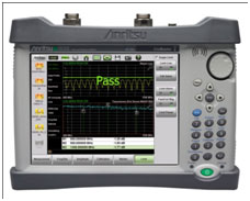
Handheld VNA is having Spectrum Analyzer combination version as well. This means user does not need to carry Spectrum Analyzer and VNA for various measurements. He can perform all Spectrum and VNA measurement with single unit. This saves cost and time.
Anritsu launched various models of Shockline VNA during 2014. This is patented technology. This series of VNA have better cost performance ratio. Many applications does not need a high cost VNA and simple measurement can be carried out using Shockline VNA under production , R&D stage.
Vector Star™ is most power VNA from Anritsu for all R&D and critical applications.
Anritsu recently introduces Vector Voltmeter Mode with Full A/B and B/A Ratio Capability for Microwave Site Master

The Site Master S820E combines leading-edge performance, functionality, reporting, and durability to meet the most demanding field testing requirements. It is the only handheld field solution with a VVM option specified to 40 GHz, – 20x more than current alternative solutions. When using the A/B and B/A ratio capability, a unique Auto-tune feature allows the S820E to successfully lock onto an external reference source signal that can be as much as ± 100 kHz away from the selected tuned frequency, without having to widen the measurement IFBW or establishing common 10 MHz reference time-base signals. Input sensitivity for either the A or B reference receiver ranges automatically from +5 dBm to –60 dBm, surpassing the range of traditional vector voltmeters.
To save valuable time in the field and prevent poor measurements that lead to incorrect data, a Reference Signal Detection message advises users when the instrument successfully locks onto the external source signal when making A/B and B/A ratio measurements. The message is displayed at the bottom of the display in bright green, so it is easy for users to know when measurements can be made.
Keysight Technologies’ New ENA Vector Network Analyzer Advances Performance, Speed with Tenfold Faster Test Times
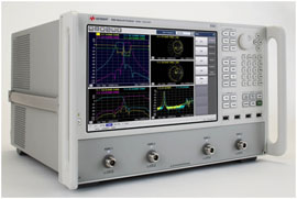
Keysight Technologies announced the E5080A ENA vector network analyzer (VNA), which offers the industry’s best combination of RF measurement performance and speed, enabling a tenfold improvement in test time. The new ENA uses the Keysight PNA- and PXI-Series software architecture, making it easier for engineers to take measurements across multiple Keysight VNAs. The ENA also offers a large color touchscreen display with fast access to basic measurements.

The E5080A sets the new standard in RF component testing for R&D and manufacturing environments. The E5080A offers comprehensive functionalities for measuring active and passive components such as amplifiers, mixers, antennas and cables, including balanced DUTs.
Compared to the popular E5071C ENA, the E5080A offers performance advantages including more than 10 dB wider dynamic range (typically 147 dB) and up to 10 times faster measurement speed in real-world test scenarios. These enhancements improve precision and throughput in the testing of RF components such as filters with deep rejection bands.
Keysight is the first VNA vendor to provide a software platform that spans benchtop and PXI-based VNAs. This universal platform uses the best attributes and capabilities of the ENA and PNA families and delivers familiar functionality across all Keysight VNAs. With the new touch-based GUI capabilities, including tabbed softkeys and drag-and-drop operations, the E5080A streamlines measurement flow and helps engineers get better results in less time.


