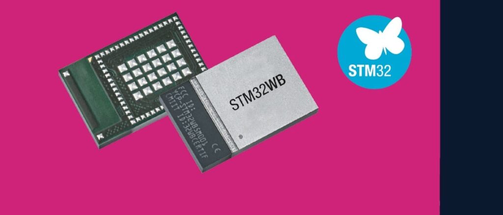
How can teams create a Bluetooth LE, Zigbee, or Thread application when low volumes may not justify the investment? The answer partly resides with the STM32WB55MMG, the first STM32 module. It includes an antenna, crystals, and everything else necessary to use the embedded RF present on its STM32WB55 microcontroller. It thus represents a new solution for engineers that struggle with costs or design considerations. Hence, by simplifying access to certification, the STM32WB55MMG dramatically reduces the time to market. Similarly, its hardware flexibility ensures that smaller teams aren’t overwhelmed by inherent complexities.
A current paradox is that while Bluetooth LE, Zigbee, or Thread applications are widespread, releasing them to market can get excruciatingly complex. BLE is so accessible that it serves as a teaching support for first-year engineering students. Indeed, the technology is far more accessible than it was ten or 15 years ago. Yet, companies may still face regulatory or design hurdles that quickly add up, especially for low-volume products. What does one say to a manager complaining that the time, human, and monetary investments are too high for a product that won’t exceed 50,000 units? The STM32WB55MG provides new answers.
STM32WB55MMG: Shifting the Cost-Benefit Analysis
Solving the Certification Conundrum
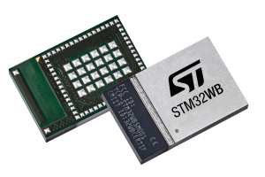
The STM32WB55 remains the only dual-core Cortex-M0+ and Cortex-M4 microcontroller with an embedded wireless transceiver. The component supports Bluetooth LE 5.2, Zigbee PRO/ZCL 3.0, Thread, and proprietary protocols. Moreover, thanks to the P-NUCLEO-WB55 development board and our software solutions, designing a custom board is relatively straightforward. Yet, certifying such a design can get challenging, especially for smaller teams. Some members of the ST Partner Program can help, but the task can still be daunting, especially if a company only makes low-volume products. Spending tens or even hundreds of thousands of dollars in testings and filings can get discouraging.
The monolithic architecture of the STM32WBMMG is a unique solution to this problem because ST took care of its certification. By design, the system we validated stays untouched inside the module’s packaging. Hence, the certification process will only focus on minor points of implementation since the regulatory bodies already approved the major hardware implementation. Moreover, we secured a lot more than the traditional FCC (USA) and CE (European Union) certifications. The STM32WB55MMG also received validations from TELEC and MIC (Japan), CCC (China), IC and ISED (Canada), KC (South Korea), and BSMI (Taiwan). Hence, exporting a design worldwide became a lot simpler, which further increases the return on investment.
Overcoming Design Complexity
Engineers may also face serious design challenges. A couple of years ago, an ST Partner explained how a Bluetooth LE product often demanded external expertise. Tuning the antenna and optimizing the RF is complex, and small teams may have to outsource the process. By using the STM32WB55MMG, engineers no longer have to worry about it. ST did all the work so they would not have to. Additionally, it is possible to use the new device in 2-layer and 4-layer PCBs, thus offering greater flexibility. Indeed, for configurations that don’t require all of the module’s features, using a 2-layer PCB helps reduce costs. On the other hand, designers looking to create more powerful applications will appreciate that we are using a full STM32WB55, which means enjoying the same peripherals, security features, and access to tools like STM32CubeMX to jumpstart projects.
STM32WB55MMG: Focusing on Features Rather Than Implementation
Inspiring Reference Design
Now that the STM32WB55MMG offers engineers a new cost-benefit paradigm, their next challenge will be to demonstrate a tangible path to market. Teams must also explain how the component will fit into the final product. Hence, ST is announcing the upcoming release of the STM32WB55MMG-DK, which should arrive this quarter. The Discovery Kit will serve as a reference design, meaning that engineers can get inspiration from its schematics. It will also show managers that the module doesn’t compromise the overall footprint. Indeed, in some instances, integrating so many components inside a package can take significantly more space than a custom approach. However, the STM32WB55MMG uses an LGA86L package measuring only 7.3 mm x 11 mm, thus ensuring designs remain compact. As a result, having such a reference design further reduces the time to market already shortened by using the module itself.
Visionary Applications
The STM32WB55MMG-DK board is also a reflection of our desire to increase the accessibility of all the microcontroller’s features. Indeed, engineers know that it can be hard to go from a list of specifications on a data sheet to taking advantage of the technologies available. Hence, the Discovery Kit will have a myriad of sensors, an LCD, external memory, and more. It will thus be a one-stop-shop to experiment with security features like Secure Boot and Secure Firmware Install. Developers will also be able to test the QuadSPI interface to utilize external Flash better quickly. And the display will help evaluate the integrated LCD driver.
The development board is highly symbolic because it serves as a technological demo for Bluetooth IoT application, rather than a simple window into the STM32WB55MMG. Too often, teams underestimate what they can accomplish because coming up with a proof-of-concept is too difficult. Thanks to the upcoming STM32WB55MMG-DK, they have all the resources to go far beyond basic feature-sets. For instance, ST will also update its FP-AUD-BVLINKWB1 Function Pack to offer a pre-compiled binary for the new Discovery Kit. The application streams music and voice over BLE to simulate a smart speaker. Engineers can, therefore, better envision the creation of modern and compelling products without fearing the inherent challenges that come with an RF implementation.
Click Link – https://blog.st.com/stm32wb55mmg/


