Soldering Technology – The first engineering technology !!!

From the Bronze age Soldering is giving its utility by the pieces of jewellery, tools and weapons and the goldsmiths of ancient Egypt knew how to join gold more than 5,000 years ago. “The age of Soldering “ came when tin was discovered as a soldering metal – and that was 4,000 years ago! The most impressive achievement of Soldering can be named to Ancient Romans, they soldered 400 km long water pipes made of lead with seams which could withstand 18 Atm and conjured up stoves and tubs made of bronze. From then on, the world’s soldering technology was on its way upwards.
Basic Soldering Techniques Principal :
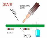
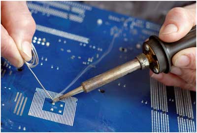
Soldering is a technique in which two or more metal items are joined together by melting and flowing a filler metal (solder) into the joint, the filler metal having a lower melting point than the adjoining metal. Soldering differs from welding in that soldering does not involve melting the work pieces.
Flow of all soldering process – Soldering medium
Solder, as a word, can be used in two different ways. Solder, refers, to the alloy (a substance composed of two or more metals) that typically comes as a long, thin wire in spools or tubes. Solder, the verb, means to join together two pieces of metal in what is called a solder joint. So, we solder with solder!
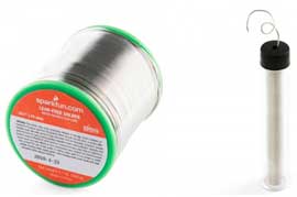
Soldering materials (Soldering medium) are available in many different alloys for differing applications. Some of the applications of solder alloy are:
- The eutectic alloy of 63% tin and 37% lead – Electronic Assembly
- Tin – Lead 60/40 alloy : Plumbing, mechanical assembly, and other applications
- Tin – Zinc Alloy : Aluminium connection
- Lead – Silver Alloy : For temperature higher than room temperature
- Cadmium – Silver Alloy : for strength at high temperatures
- Zinc – Aluminium Alloy : Aluminium and corrosion resistance
- Tin – Silver Alloy : Electronics
- Tin – Bismuth Alloy : Electronics
Leadout of Soldering
Traditionally, solder was composed of mostly lead (Pb), tin (Sn), and a few other trace metals. This solder is known as leaded solder. But is was discovered that Lead is very hazardous to environmental health and fumes generated during leaded soldering process can cause harmful diseases like cancer to operator. Unfortunately, lead is also a very useful metal, and it was chosen as the go-to metal for soldering because of its low melting point and ability to create great solder joints.
With the adverse affect of leaded solder, introduction of regulations such as the European RoHS (Restriction of Hazardous Substances Directive) can to picture.
Global Lead-Free Regulations & Exemptions:
On February 13, 2003, lead-free became a law in the European Union (EU), with an implementation date of July 1, 2006. From that date on, no electronic products (except those with exemptions) can be made in or shipped to the EU if they contain lead.
In some products, lead is exempted by RoHS. For example, lead in solder for servers, storage and storage array systems. Lead in solder for network infrastructure equipment for switching, signaling, transmission as well as network management for telecommunications. Lead in electronic ceramic parts such as piezoelectronic devices. Lead in high-melting-temperature-type solders such as tin-lead solder alloys containing more than 85 wt percent Pb.
But there are exemptions to RoHS, such as – monitoring and control and medical equipment as of their complexity, reliability and requirements of long design and life cycles.
- Copper alloy containing up to 4% lead by weight is permitted.
- Lead in high melting temperature type solders (i.e. lead based solder alloys containing 85% by weight or more lead).
- The servers, switches, routers, cell sites and other telecommunication equipment that constitute the global Internet and phone systems are exempt from lead content restrictions.
- Cadmium in Solar panels – Cadmium telluride (CdTe) thin-film PV modules in photovoltaic panels are explicitly allowed by RoHS to contain unlimited cadmium, even though cadmium is restricted in all other electronics. The solar panel exemption was in the original 2003 RoHS regulation and it was further extended on May 27, 2011.
- Limited amounts of mercury in fluorescent and other light bulbs where it is essential to their functioning comprise RoHS
The Chinese Government recently began formalizing a version of RoHS, with a lead-free implementation date of July 1, 2006. The final law was scheduled to be published at the end of 2003.
With the new research coming up RoHS products that are currently exempt from compliance are expected to be RoHS compliant. e.g. computer servers.IBM has announced a RoHS solution for high lead solder joints once thought to remain a permanent exemption. The lead-free packaging technology ” Test and measurement vendors, have also started to produce RoHS-compliant products, despite devices in this category being exempt from the RoHS directive
Lead-Free Solder
The usage of LF (Lead-Free) Solder was slow for almost a decade until Japan started a movement for lead-free consumer electronics in about 2000. With a viable lead-free alternative and a tight-knit electronics manufacturing association that enabled a broad industry-wide shift, Anderson said the Japanese push for lead-free consumer electronics soon spilled over to other nations, including a 2006 European Union law banning lead in electronic components.
Given the international nature of the electronics industry, lead-free consumer electronics manufacturing became global by proxy, marked by a noticeable growth in lead-free solder licensing rates. Between 2008 and 2011 alone, royalties generated from lead-free licenses increased 105 percent.
Lead-free solder’s recent achievement reflects the key role it’s playing in helping companies both efficiently and responsibly manufacture the popular electronic products that have revolutionized communication in the 21st century.
Lead-free Solder Paste and Products
Lead-free solder is very similar to its leaded counterpart, except, as the name states, it contains no lead. Instead is made up of mostly tin and other trace metals, such as silver and copper. This solder is usually marked with the RoHS symbol to let potential buyers know it conforms to the standard.

The RoHS directive is aimed at restricting the use of 6 hazardous materials in the manufacture of electrical and electronic devices as follows:
- Lead
- Mercury
- Cadmium
- Hexavalent Chromium
- Polybrominated Biphenyls
- Polybrominated Diphenyl Ether
The result of this directive on the electronics industry varies greatly depending on product end use and target sales market. The overall supply chain from individual components to bare printed circuit board manufacturing has shifted from a predominately tin-lead alloy based market to one that caters almost exclusively to lead-free finishes. The result has been limited supply, and in some cases, complete elimination of tin–lead plated components. This has, in effect, forced manufacturers to make design and process changes on products that were traditionally tin-lead based.
The primary difference between tin/lead and lead-free solders, from a rework and repair standpoint, is the temperatures required to form a proper intermetallic bond. For the most widely used tin/lead alloys such as Sn60 Pb40 or more commonly Sn63 Pb37 (eutectic), the melting point is 361°F (183°C). The most commonly used lead-free alloy, Sn96.5 Ag3.0 Cu0.5, commonly referred to as SAC 305, has a melting point of 422°F (217°C) to 428°F (220°C). The resultant increase in melting point will have the effect of reducing the overall process window and can change the traditionally accepted appearance of the finished product.
One of the major differences between lead-containing and lead-free solder pastes in soldering technique is the “flow” of the solder in its liquid state. Lead-containing solder has a lower surface tension, and tends to move slightly to attach itself to exposed metal surfaces that touch any part of the liquid solder. Lead-free solder conversely tends to stay in place where it is in its liquid state, and attaches itself to exposed metal surfaces only where the liquid solder touches it. This lack of “flow” — while typically seen as a disadvantage because it can lead to lower quality electrical connections — can be used to place components more tightly than they used to be placed due to the properties of lead-containing solders. For example, Motorola reports that their new RoHS wireless device assembly techniques are “…enabling a smaller, thinner, lighter unit.” Their Motorola Q phone would not have been possible without the new solder. The lead-free solder allows for tighter pad spacing
Lead – Free soldering techniqie, increases peak temperature, and increases complexity matrix of temperature, thickness and volume for lead-free components are added. Also, the time within 5°C of actual peak temperatures is changed to 15 seconds.
Lead – Free Impact on PCB & Components
There are four groups of components in EMS:
- Discrete (chip resistors) packages
- SMT leaded (plastic quad flat pack) packages
- BGA, Balled (plastic ball grid array) packages
- Plated through-hole (PTH) packages.
For SnPb-leaded components, surface finishes mostly have SnPb plating. For lead-free components, the leading surface finishes are -Sn plating for SMT leaded components for short life-cycle (5 years or less) applications and matte-Sn plating with Ni-barrier under-layer for long life-cycle products; Sn3 wt percent Ag0.5-1 wt percent Cu for solder-balled components; and either Sn-plate or Sn-dip for PTH components.
Building Better Solder for New Markets and Tougher Tests
With lead-free solder now an industry standard, researchers have been working on next-generation versions that overcome certain flaws in the original formulation – for instance, the tendency for solder joints to become brittle over time from prolonged exposure to high operating temperatures. These improvements may open new avenues for adoption. A growing interest in lead-free products in the U.S. military also can open new markets for lead-free solder and soldering techniques in the coming years. predicted is a very new future, where electronic industry completely eliminate lead from EMS process.
GREENPOXY 55
Going to the nest generation of Green, Electronic Assembly Process, GREENPOXY 55 is an epoxy system formulated with a high percentage of biomass carbon content. The formulation of an epoxy system is a compromise between various usual characteristics. ‘Traditional’ organic chemistry offers a vast choice of raw materials, while ‘green’ sourced raw materials are still rare. GREENPOXY 55 is an epoxy system with a single hardener, where 55% of the molecular structure is of plant (biomass) origin. It thus contains 55% of ‘green’ carbon.
The hardener GP 505 follows the same logic and contains carbon coming from biomass. GREENPOXY 55 has an average viscosity enabling the manufacturing of various different parts. Applications are:
- Hand lamination for tooling or industrial parts
- RTM processes (infusion, injection…)
- Filament winding
- Hot or cold press
- Casting
- Bonding
Temperature & Humidity for an Electronics Assembly Facility
For every electronic Assembly it is very important, to have a temperature and humidity controlled environment for any electronics assembly environment. Ideally, the temperature would be in the range of 70-77 F and the relative humidity would remain in the range of 35-65%. Lack of humidity and temperature control can influence defect levels in wave soldering and SMT applications.
- Low humidity: Solder paste solvent evaporates quicker than expected, causing the paste to dry out. This creates poor release from stencils and insufficient solder joint defects.
- Low temperature Paste viscosity increases, creating poor printing behavior (rolling, release, etc.). This can cause insufficient solder joint defects.
- High humidity: Solder paste accepts water and may begin to slump, creating additional bridging defects. Solder paste accepts water and may exhibit poor coalescence, resulting in solderballing defects. Moisture-sensitive components stored in this area will have shorter shelf life, possibly creating defects and/or damage to the components during processing. Excess water absorbed by the entire system (boards, components, paste) can out-gas during reflow and increase the size and incidence of voiding underneath BGA components.
- High temperature: Solder paste viscosity decreases, possibly creating an excess of paste smearing, slumping, etc. This can cause bridging or solderballing defects. Higher temperatures in the factory induce extra oxidation of solder, boards and components prior to soldering, meaning that solderability can be compromised with higher factory temperatures.


