 In addition to the increasing penetration of EVs and HEVs, the growing demand for advanced driver assistance systems (ADAS) and proliferation of high-end in-car infotainment systems are among the key factors fueling the increase of electronics in cars. One of the automotive segments that are expected to exhibit high growth is the ADAS, mainly due to stringent safety regulations in modern cars. ADAS, as an array of systems and subsystems that incorporates electronic components such as sensors, microcontrollers and software under one roof, is forecast to register market growth of 14.9% CAGR from 2015– 2020, according to research firm IndustryARC.
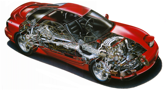
As the amount of electronics that go into a car increases, the car is becoming less of a mechanical thing consisting of a few electronics and more of a computer with wheels. The electronics’ share of vehicle value for a state-of-the-art automobile is already at 40% for traditional, internal combustion engine cars, and it could reach 75% for electric or hybrid electric vehicles. This percentage value will definitely rise in the next few years. Automotive electronics rose by 7.3% in 2014 to about US$205 billion and will continue to grow at the same growth rate to 2020, at close to US$315 billion based on a report by Research and Markets. The advanced driver assistance systems (ADAS) market will have a 14.9% CAGR from estimated revenue of US$39 billion in 2015 to US$78.2 billion in 2020, according to Industry ARC. According to New Venture Research, of the $91.2 billion worldwide automotive electronics assembly value in 2014, 86% was done in-house by the OEMs; 1% by the ODMs; and 13% by the EMS providers. The automotive industry continues to grow rapidly as a high-growth market for EMS providers as it transitions steadily from mechanical to electronics. Indian automobile machines are evolving interestingly. Not only cars manufacturing but also EMS companies are considering automotive jobs. In line of such requirements SMT industry is here to serve special machines for Automotives. The most curtail module of a typical SMT process transformed for automotive application is the inspection in-view to special components and specifications of an automotive card. This exclusive study will bought to you some dedicated application Inspection machines for Automotive applications.
In the automotive electronics industry, the challenges regarding 100% functionality of all components are growing constantly. That means maximization of quality assurance and inspection depth in production processes. In connection with new innovative components and production technologies, this requires permanent development of inspection technologies. Manufacturers experience an increasing transition from “inspecting” to “measure,” especially when it comes to different kinds of application (e.g., distance measurement of components or spatial allocation of components [3D measurement]). Furthermore, Industry 4.0 is on the horizon: requirements according to different MES (manufacturing execution systems) connections have established themselves in the meantime to an extremely important part of the overall system. There is a dramatic shift occurring in the manufacture of automobiles. Electronics are taking over in every aspect, even to the point of connecting the car with the Internet and even other automobiles. The implications and challenges for the manufacturer are far reaching. Some of the latest developments in AOI technology aimed at addressing the high-reliability requirements of automotive electronics, the use of 3D measurement in electronics manufacturing has brought a significant development of AOI systems. AOI suppliers have to develop the application possibilities of the 3D measurement systems, starting from simple component recognition to co planarity measurement and determination of solder volumes. Increasing the speed of inspection and higher detail recognition of smallest errors will constantly be a challenge. Apart from the integration of 3D measurement methods, in the foreseeable future no revolutionary advancements in AOI technology are to be expected.

OMRON Automation Pvt Ltd
Hemant Gangurde, Manager – Sales, AOI Optical Inspection, OMRON Automation Pvt Ltd
AOI – Automated Optical Inspection is one of the very important needs for PCB manufacturing/assembly process for achieving the fastest quality production output. AOI and SPI Inspection systems are a great support for the Automotive Safety & Accessories application PCBs to meet their real improved quality on a continuous basis. The AOI technology provided by OMRON meets requirements of all types of automotive customers. The brand is recognized as the best high-end post reflow & wave AOI. It has strong Inspection capabilities especially in the field of solder inspection and data collection. OMRON AOI division offers the following products:
- AOI – Offline & Inline 2D AOI – ( Model – RNS )
- AOI – Inline 3D AOI ( Model – S Series )
- SPI – Inline 3D SPI ( Model – VP Series )
- X-Ray – Inline 3D X-Ray Inspection ( Model – X Series)

Mrs. Kumud Tyagi- Vice President, Bergen Associates Pvt. Ltd.
Modus AOI S1-IDA from MODUS, Germany:
The double sided AOI system is designed for simultaneously inspection from top and bottom. The system has two multi-LED illuminated scanner units as well as the patented special lenses which generate parallax free pictures. It includes modus control units with the modus software. The ASYS transport module provides a system length of 1500mm/1590mm (59.1 in./62.6 in.) Two transport segments with 1060 mm and 530 mm [41.7 in./20.8 in.]. Few characteristics are, Double system for double-sided simultaneous inspection printed circuit boards, Combination of diverse inspection tasks such as SMD placement, THT solder joints, conformal coating and full screening for solder bead (solder balls) and lost components from top only, Capture of barcode and data-matrix codes in any position and quantity on the multi PCB, Simultaneously display of all results of both sides.
Challenges with AOI
Many inspection challenges exist when inspecting SMT assemblies. The root cause of some of those challenges are imaging related, while others are inspection algorithm related. The addition of 3D imaging to the AOI market has solved some inspection deficiencies present in 2D AOI systems by providing the much-needed height information to the inspection algorithms to find height related errors like lifted leads and package co-planarity. However, accurately imaging in 3D the surfaces of SMT assemblies presents additional challenges to the inspection system. For over 15 years, vendors have offered 3D inspection to the Solder Paste Inspection (SPI) market, yet the AOI market has only recently begun to benefit from mainstream 3D inspection. This delay was overcome primarily due to breakthroughs in sensing and computing technology. Following is a sampling of obstacles to high quality 3D inspection. Most modern 3D systems rely upon some form of triangulation sensing; usually phase profilometry, to obtain the speed and accuracy necessary for SMT production.
Another challenge befalling 3D AOI inspection systems involves all the additional image acquisition on processing required to keep up with product speeds. It is common for the number of images required to obtain information for height reconstruction be an order of magnitude higher than the number of images necessary to perform 2D only inspection. The amount of image processing also grows commiserate with the number of images taken and additional inspection tasks performed. In some factories, 2D AOI inspection is barely keeping up with tact times. For others, adding 3D inspection pits the process and quality engineers in conflict with the production managers responsible for line utilization and production capacity. The compromise is choosing a strategy to determine points to degrade inspection performance by inspecting with 2D only. These decisions will be made on a field of view level to reduce the number of acquired images further complicating and compromising the inspection capability. A solution that eliminates the need to compromise inspection quality to meet production demands is preferred.
|
In 2D inspection, almost every attribute can be described in dimensions of X and Y. There may be some shapes that are difficult to represent with straight lines and curves, but most objects conform to those constraints in 2D space. In 3D, the extra height variable presents an added complexity in describing surfaces and it does not take long for the height function to become mathematically complex. In SPI inspection, this shape analysis complexity is addressed by presenting the relevant summary measure of volume. This same volume summary measure can work for some AOI inspection types like THT and lead toe solder joint measurement, however, visible volume is not a true indication of a good solder joint. There could be strong heal wetting pulling a majority of the toe solder away, or the right amount of solder, but no wetting as in a cold solder joint.
3D AOI for Automotives
Driven by the continued decrease in the size of electronics packaging, combined with the increase in density, there is a critical need for highly accurate 3D inspection for defect detection. Using multi-view 3D sensors and parallel projection, it is possible to capture more of the board at a faster rate as compared to serial image acquisition which is more time consuming. Precise 3D image representation can then be generated using sophisticated fusing algorithms that take the multiple captured images and fuse them into one precise 3D image. The result is high speed 3D inspection. Multi-reflection suppression (MRS) technology enables highly accurate 3D measurement by meticulously identifying and rejecting reflections caused by shiny components and reflective solder joints. MRS algorithms use a very rich data set from multiple cameras at every location. Combined with sophisticated algorithms that fuse the image data from multiple cameras, multiple reflections are effectively suppressed. By contrast, 3D sensing solutions that use triangulation illumination without MRS run into measurement accuracy issues since solder joints create multiple reflections that can corrupt height image. This technology is a key building block for achieving high accuracy at production speed in an Automated Optical Inspection (AOI) system. New capabilities in AOI systems with the advent of 3D imaging will increase inspection confidence in users that have been elusive until now. This will enable improved quality and understanding of electronic assembly process which will improve yield and manufacturers’ profits. In summary 3D AOI provides:
1) Zero Defects and a greater production speed.
2) Minimizes assembly, testing and measurement errors.
3) Short time to market
Conclusion
With invent of advance and hybrid cars, the manufacturing became much sophisticated and virtual, making AOI or inspection a very important aspect of whole manufacturing process. Visualizing the trends, many AOI, X-Ray and specified application machines are available in market to make sure your car is tested and inspected 100% at every stage of manufacturing.


