With the largest no of electronics items consumed by Indian market, India has a very large industry base of Electronics items, but when we talk about semiconductor inside, we import 95% part of it. With the highest level of
intelligence man-power & great level of natural resource, why we are not fabricating Semiconductor devices in-house. What are the obstacles to set-up a semiconductor foundry in India. Lets talk about some of the factors affecting semiconductor fabrication in India.

The semiconductor industry in India is growing at a rapid rate as compared to the world average, influenced by increasing demand of electronic gadgets & Industrial expansions. Moreover, for the high tech gadgets available today requires higher power than reforms designing of semiconductor part of the device. Making a gadget trendy, resizes the chip inside. To address these challenges, existing manufacturing infrastructure is required to be upgraded and new full-flashed manufacturing is required in local Indian market. The wearable & smart electronics trend at our footstep future will influence entire semiconductor industry. Global semiconductor industry will be driven largely by macroeconomic development and technological advances. The industry has been witnessing an increasing demand from the BRIC (Brazil, Russia, India, and China) economies due to increasing end-use electronic product demand. Global semiconductor industry is expected to witness a CAGR of 4.3% over the next five years and reach an estimated $394 billion in 2017. India industry can wholly cater this demand in all aspects of intelligence, Man-power, raw material and natural resources and thus has a great potential to evolve as a semiconductor manufacturing hub. The roadmap will require the country to makes necessary investments in infrastructure and education. There is a need to boost the electronic design and manufacturing in India, promote product development, nurture startups and introduce a level playing field at different points in the entire electronic ecosystem. These efforts will in turn help foster growth. All these would require rigorous efforts from various stakeholders involved in the entire ecosystem and continuous encouragement from the government is needed to pull investors to make to large investments. Also, as per Government of India the bill of Import of electronics items in India will exceed that of petroleum by 2020, this factor clearly illustrates the significance of Indian semiconductor fabrication facilities. The cost of incentives for building FABs in India is likely to be large. A simultaneous

focus on formation of local semiconductor design and product companies along with the FAB seems to be key to success. Local product companies become loyal customers, bring a steady source of revenue and are more profitable than global MNC customers. Global customers extract every bit of concession reducing the profit; moreover, they would migrate to a FAB in a different geography if more incentives are offered. India, as a destination for semiconductor foundries (fabs), has both advantages and drawbacks. Fab close to the design location can be useful, however, the $2-$3 billion price tag is prohibitively high, not to mention periodic up-gradation costs. Moreover, worldwide overcapacity is already squeezing the bottom lines of the foundries. Even if the huge domestic market can outweigh the capacity concerns, poor infrastructure and lack of experience makes it an uphill battle for Indian fabs.
India has been a service oriented market. It needs to transform itself into product oriented market. And for that there is lot more which needs to be done by the Government, by business leaders, entrepreneurs and the people in general, to change the mindset to take up ownership. It needs a positive vibrant environment where people and specifically entrepreneurs are able to see the real value created by their suppliers and employees, and reward them, and in return create greater value for themselves. It must be a win-win situation.
Setting-up a Semiconductor facility in India.
A Long Term Plan – As Foundry setup is highly Capital intensive, it must be supported with a solid long term plan and financial backing. This backing is required from the entrepreneur & the government both.
Fiscal Sustenance – In text of Indian Government as tax holiday, subsidy, zero duty, financial investment etc. will play an important role in promoting the Fab along with the semiconductor industry in India; this will put further pressure on already large Fiscal Deficit. A stubbn financial system is required to bought in picture.
Support Infrastructure – This is a very important aspect which needs to be looked at for smooth running of the Fab. A world class, sustainable infrastructure, as required by a modern Fab be provided, with swift transportation, large quantity of pure water, uninterrupted electricity, communication, pollutant free environment etc.
Government Policy – This is one of the most important factors for such a massive step to be taken. The policy (that includes all kinds of subsidies, which may be tapered down in future with due conditional clauses) taken up now must be valid and stable for at least 10 to 15 years irrespective of which party is in power.
Obstacles & Challenges.
1. Huge Investments involved
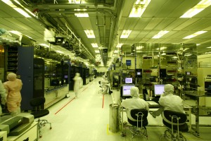
Semiconductor Fabrication facility requires many expensive devices to function. Estimates put the cost of building a new fab over one billion U.S. dollars with values as high as $3–4 billion not being uncommon, as per TSMC, Taiwan. The central part of a fab is the clean room, an area where the environment is controlled to eliminate all dust, since even a single speck can ruin a microcircuit, which has features much smaller than dust. The clean room must also be dampened against vibration and kept within narrow bands of temperature and humidity. Controlling temperature and humidity is critical for minimizing static electricity. The clean room contains the steppers for photolithography, etching, and cleaning, doping and dicing machines. All these devices are extremely precise and thus extremely expensive. Prices for most common pieces of equipment for the processing of 300 mm wafers range from $700,000 to upwards of $4,000,000 each with a few pieces of equipment reaching as high as $50,000,000 each (e.g. steppers). A typical fab will have several hundred equipment items. Complex tools and equipment are required to test quality and move silicon from location to location within the ultra-clean confines of the plant.
2. Semiconductor Fabrication is a volume production facility rite from the starting.
Semiconductor fabrication is a volume game rite from the start-up. Even if the portfolio is of some very few products, manufacturer has to maintain a large volume production facility to support volume orders that will result in very high investment in the beginning, as the utilities required are very critical and normally couldn’t be supported from Indian market. In semiconductor fabrication it is required that a high volume production is required to be maintain so as to meet the increasing demand of the marketplace, but at the same time, a strong financial backing as Indian market is very much uncertain about financial fluctuations. One has to go for volume, which requires a lot of capital investment, because you need utilities that are critical.
3. Semiconductor Fabrication will require cheap but skilled labor.
Semiconductor manufacturing a large labor is required, well-educated yet cheap. Of-course there is no problem of man-power in India, but that to skilled is a consideration. India is the world’s 2nd largest population country and our un-employency levels are also very high, that makes cheap labor available in India very easily, but we do not have a wel- education manpower available with us at a very large numbers to be work in semiconductor fabrication facilities especially at labor level. Labor available in India are mostly unliterate especially when we talk about a semiconductor fabrication facility that will be quite far from a city or a education hub, the local labor available at the site, could be sufficient in number & cheap as wel, but may not be qualified & skilled to handle sensate process like Semiconductor fabrication. Company setting – up the fabrication plant, has to train the workers in the facility for the sophiscated process evolved in the process, very high cost machinery involved, critical raw material & sensitive finished parts used in the process & addition shop floor requirements of the facility. That will definitely not going to be a very easy thing and will add to cost & facility staff of the semiconductor fabrication facility.
- 4. Vey High end world –class machinery involved.
Semiconductor fabrication is a multiple-step sequence of photolithographic and chemical processing steps during which electronic circuits are gradually created on a wafer made of pure semiconducting material. Various compound semiconductors are used for specialized applications. The entire manufacturing process, from start to packaged chips ready for shipment, takes six to eight weeks and is performed in highly specialized facilities referred to as fabs. Some of the processes in the semiconductor fabrication can be named as, Wafer processing, that includes, Wet cleans, Photolithography, Ion implantation (in which dopants are embedded in the wafer creating regions of increased (or decreased) conductivity), Dry etching, Wet etching, Plasma ashing, Thermal treatments by, Rapid thermal anneal, Furnace anneals & Thermal oxidation, Chemical vapor deposition (CVD), Physical vapor deposition (PVD), Molecular beam epitaxy (MBE), Electrochemical deposition (ECD), Chemical-mechanical planarization (CMP), Wafer testing, Wafer backgrinding (to reduce the thickness of the wafer so the resulting chip can be put into a thin device like a smartcard or PCMCIA card.). The next step will be Die preparation, by process flow, Wafer mounting & Die cutting. Then it is IC packaging, done by Die attachment, IC bonding, Wire bonding, Thermosonic bonding, Flip chip, Wafer bonding, Tab bonding and IC encapsulation by Baking, Plating, Laser marking & Trim and form. The final step is IC testing. One or all processes mentioned used very high end machines from global companies making setting – up a semiconductor fabrication facility a huge infrastructure investment. Not a only a huge initial investment, every changing trends & innovation in electronics is redesigning the electronics inside, thus the up-gradation of the infrastructure became a must requirement to survive in market.
- 5. Requirement of very specific raw materials.
From a value-chain perspective, the foundries take in raw materials, such as silicon, gases and many more. Silicon, is a very basic & most commonly used raw material use in semiconductor fabrication, apart from silicon , Germanium & Gallium arsenide and Silicon carbide are also sometimes used in fabrication process. The sand used to grow the wafers has to be a very clean and good form of silicon. For this reason not just any sand scraped off the beach will do. Most of the sand used for these processes is shipped from the beaches of Australia. This fact adds to the trouble of the fabrication facility as they have to either import very basic utility of the fabrication, or add an additional floor in the facility to clean-up the local sand available in India. Apart from Silicon, numerous types of chemicals & gases are involved in semiconductor fabrication that are not till now available in India and has to be imported.
- 6. Uncertain Indian market
Further to that we all know that the Indian market is very uncertain about financial downfalls, and highly influenced from Western market, this facts adds to be trouble of semiconductor fabrication in India as any fluction or changing trend in world market can change their entire demand-supply structure and could disturb financial structure. Fact is that a semiconductor fabrication facility in India cannot independently rely on Indian customers for their entire sales structure. They have to maintain overseas customer base to balance influctions from Indian market due to market trends, government policies etc. This factor sorts out the local companies from the list of semicon may setup their fabrication in India, and the prospect left to multinational companies itself.
- 7. Customer requirements are changing, and change the electronics inside.
High end setup, utilizing skilled labor and expensive equipment to fabricate finished semiconductor products on behalf of a customer. Indian customers are typically either an Integrated Device Manufacturer that produces goods for the end-customer and have their own manufacturing capability, or a fab-less (fabrication plant-less) Semiconductor Company. Fab-less companies are dedicated to the design of IC’s, and do not have any internal manufacturing capability due to the high startup and maintenance cost. As a result, they turn to the foundries to produce the finalized product they have designed. The customer trends changes every day, and it is a great task for the fabrication facility to manufacturer new devices on very small targets timelines. This fact illustrates the need of a very high-end R&D set-up in the semiconductor facility & capability of the machines to change the process flow as per the modified package. One more factor is associated with this point is this, fabrication people cannot plan long term production schedule of devices, as they have to keep track of market requirements & customer demand.
- 8. Disposable of Hazardous Waste
Many toxic materials are used in the fabrication process. These include, poisonous elemental dopants, such as arsenic, antimony, and phosphorus. Poisonous compounds, such as arsine, phosphine, and silane. Highly reactive iquids, such as hydrogen peroxide, fuming nitric acid, sulfuric acid, and hydrofluoric acid. Similarly the waste of a semiconductor plant could be hazardous, may be in form of gases or liquid or solid. Decomposition of this kind of waste in open or in natural resources like cannels can cause serious damage to people line nearby. At this satge government concern is required to provide the facility right guidelines & suitable medium to filter the waste & dispose them in the recommended medium. But till now government of Indian is not offering any such dedicated industrial area for semiconductor fabrication that is safe & suitable from disposal time of view. So the whole responsibility of decomposing this waste comes to the semiconductor company, adding the infrastructure & financial requirements.
- Infrastructure Requirement
Supply of quality uninterrupted power supply is very critical in semiconductor fabrication. There would be very few places in India where one can generally get power without any problem. And relying on generators or any other kind of power source is not possible for fabrication process. Water availability in pure format is also necessary, fab is going to use any normal water to double, triple reverse osmosis, purification, deionization. Government of India has to make assurance of providing this kind of infrastructural utilities on uninterrupted basis to the facilities.
- Lack of education in Indian on Advanced semiconductor manufacturing
Indian engineers & scientist are the best in World, but our education trend is more towards software rather than core technology like semiconductor manufacturing. There is little to no institute, which are doing cutting edge work research in advanced semiconductor manufacturing such as 450mm, Graphene and nanotechnology materials, organic semiconductor etc. in India. In material science, there is practically little to nothing that institutes do in India– as they are more or less inclined to publications and not on ground breaking innovation. There is a general dis-belief in government that private entrepreneurs are there to just grab money and run away. So even today, people willing to set-up a plant cannot get even one single research grant from government institute. This factor de-motivates the young generation & industry to come for semiconductor fabrication in India.
Conclusion:
The Govt. of India has recently approved setting up of two Semiconductor Wafer Fabrication (FAB) Manufacturing Facilities in India. These FAB units are to be set up by two business consortia, with the following broad project parameters: M/s Jaiprakash Associates Limited (with IBM, USA and Tower Semiconductor Limited, Israel as partners), Project Cost: Rs 34,399 crore, Technology: 90/65/45/28 nm, Capacity: 40,000 WSPM, Location: Yamuna Expressway, Uttar Pradesh & M/s HSMC Technologies India Pvt. Ltd. (with ST Microelectronics and Silterra Malaysia Sdn. Bhd. as partners), Project Cost: Rs 29,013 crore, Technology: 90/65/45/28/22 nm, Capacity: 40,000 WSPM , Location: Prantij, Gujarat. This step is a considerable growth motivational factor towards Indian industry roadmap to become a semiconductor hub. India is the largest developing country and a one of the biggest consumer of electronics items from all over the world. the demand for electronics hardware in the country is projected to increase from USD 45 billion in 2009 to USD400 billion by 2020. To cater this requirement in-house the need & future of Indian semiconductor manufacturing is huge. Along with Govt. aid & helping policies it is important to create a favourable environment for all the investors, infrastructure and technological partner.


