
This new package will be expanded to small-signal MOSFETs, contributing to increased space-savings in a variety of offerings.
ROHM has recently announced the release of the smallest transistors in the industry. The VML0604 package (0.6mmx0.4mm, t=0.36mm) cuts size by 50% compared with conventional models, making it ideal for smartphones and other portable devices requiring greater smaller, thinner form factors.
In recent years in the electronics market, which includes smartphones and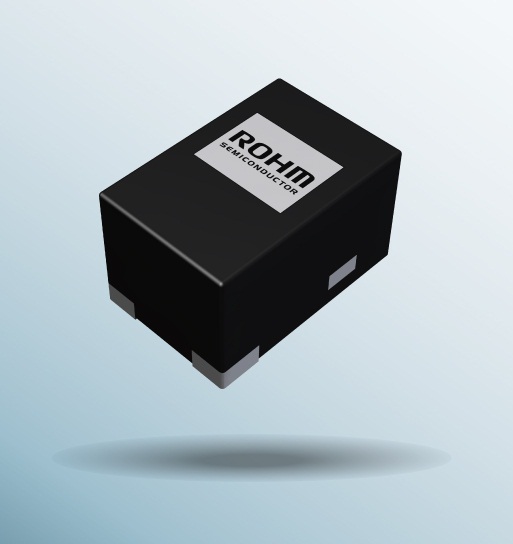
wearable devices, as the trend continues towards greater compactness
and functionality the demand grows for smaller, thinner components.
And for transistors in particular, in addition to technical challenges such as bonding stability and package processing accuracy, it has been especially difficult to increase element size, resulting in higher ON resistances and a maximum withstand voltage of only 20V. ROHM, however, was able to successfully reduce package size and ON resistance while improving voltage resistance up to 60V, providing breakthrough performance and applicability.
Pricing: 80 yen/unit (Samples)
Availability: Now (Samples), June 2014 (OEM quantities)
Key Features
1. Industry-small form factor significantly reduces mounting area
New high precision package and element processes, combined with internal structure optimization, have allowed ROHM to successfully develop the smallest transistor package in the industry, the VML0604, measuring just 0.6mm x 0.4mm x 0.36mm. As a result, mounting area is reduced 50%, making it ideal for high density applications in portable devices of all types.
This new package will be expanded to small-signal MOSFETs, contributing to increased space-savings in a variety of sets.
2. Precise 0.2mm terminal spacing improves mountability
As devices become smaller substrate mounting becomes increasingly
difficult. In response ROHM maintained a 0.2mm terminal gap that
facilitates mounting using existing equipment.
3. Ultra-low ON resistance in the world’s smallest form factor
Decreasing package dimensions places a limit on element size. As the element size decreases ON resistance increases dramatically, making it difficult to maintain the performance of conventional small-signal transistors.
However, adopting a new process element makes it possible to develop ultra-compact transistors featuring a withstand voltage of 30V along with industry-leading* 0.25Ω ON resistance (VGS=4.5V).
4. Broad lineup include 40-60V products
Higher breakdown voltages in the 40-60V range are possible, even while maintaining low ON resistance.
Terminology
・MOSFET
Transistors utilized for their high-speed switching capability.
・ON Resistance
The resistance value between the Drain-Source when voltage is applied between Gate-Source. The smaller the value the easier the current will flow, reducing loss.
 ROHM has recently announced the release of the smallest transistors in the industry. The VML0604 package (0.6mmx0.4mm, t=0.36mm) cuts size by 50% compared with conventional models, making it ideal for smartphones and other portable devices requiring greater smaller, thinner form factors.
In recent years in the electronics market, which includes smartphones and
wearable devices, as the trend continues towards greater compactness
and functionality the demand grows for smaller, thinner components.
And for transistors in particular, in addition to technical challenges such as bonding stability and package processing accuracy, it has been especially difficult to increase element size, resulting in higher ON resistances and a maximum withstand voltage of only 20V. ROHM, however, was able to successfully reduce package size and ON resistance while improving voltage resistance up to 60V, providing breakthrough performance and applicability.
Pricing: 80 yen/unit (Samples)
Availability: Now (Samples), June 2014 (OEM quantities)
Key Features
1. Industry-small form factor significantly reduces mounting area
 New high precision package and element processes, combined with internal structure optimization, have allowed ROHM to successfully develop the smallest transistor package in the industry, the VML0604, measuring just 0.6mm x 0.4mm x 0.36mm. As a result, mounting area is reduced 50%, making it ideal for high density applications in portable devices of all types.
This new package will be expanded to small-signal MOSFETs, contributing to increased space-savings in a variety of sets.
 2. Precise 0.2mm terminal spacing improves mountability
As devices become smaller substrate mounting becomes increasingly
difficult. In response ROHM maintained a 0.2mm terminal gap that
facilitates mounting using existing equipment.
 3. Ultra-low ON resistance in the world’s smallest form factor
Decreasing package dimensions places a limit on element size. As the element size decreases ON resistance increases dramatically, making it difficult to maintain the performance of conventional small-signal transistors.
However, adopting a new process element makes it possible to develop ultra-compact transistors featuring a withstand voltage of 30V along with industry-leading* 0.25Ω ON resistance (VGS=4.5V).
4. Broad lineup include 40-60V products
Higher breakdown voltages in the 40-60V range are possible, even while maintaining low ON resistance.
 |
|||
 |
|||
Terminology
・MOSFET
Transistors utilized for their high-speed switching capability.
・ON Resistance
The resistance value between the Drain-Source when voltage is applied between Gate-Source. The smaller the value the easier the current will flow, reducing loss.


