By Diarmúid Carey, Applications Engineer, Analog Devices
Question:
What active circuit protection solutions can replace TVS diodes and fuses?

Answer:
Go with a surge stopper.
Abstract
Manufacturers in all industries constantly push cutting-edge performance, while trying to balance such innovation against tried-and-true robust solutions. Designers are faced with the difficult task of balancing design complexity, reliability, and cost. One subsystem in particular, electronics protection, rebuffs moves to innovate due to its nature. These systems protect sensitive and expensive downstream electronic devices (FPGAs, ASICs, and microprocessors), requiring a zero failure rate.
Many traditional and historically proven protection methodologies—such as diodes, fuses, and TVS devices—retain their go-to status, but these are often inefficient, bulky, and require maintenance. To address these deficiencies, active, intelligent protection ICs have proven they can match the protection requirements of traditional methods but in many ways are more robust. Because of the wide range of devices available, the most difficult problem for the designer is simply choosing appropriate solutions.
To help designers narrow their choices, this article compares traditional protection methods to the ADI protection portfolio, presenting the features of these products and suggested applications.
Introduction
The increase in the amount of electronics used in all industries, and the expansion of functions handled by expensive FPGAs and processors, has elevated the need to protect these devices from the harsh environments in which they operate. Layer on top of this a need for small form factors, high reliability, and fast response to overvoltage and overcurrent surge events. This article discusses the challenges faced in many applications and why protection is needed. Traditional protection methodologies are discussed and compared to newer, alternative solutions, which offer better accuracy, reliability, and design flexibility.
Why Consider Voltage and Current Protection Devices?
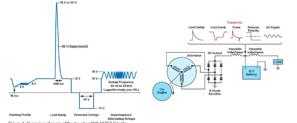
Automotive, industrial, communications, and aviation electronic systems must operate through a range of power supply surges, such as those shown in Figure 1. In each of these markets, transient events are defined in a number of industry specifications. For example, automotive transients are covered by the ISO 7637-2 and ISO 16750-2 specifications, which outline both the details of expected transients and test procedures to ensure these are consistently validated.
The types of surge events and their energy content can vary depending on the area in which the electronic device is used; circuitry can be exposed to overvoltage, overcurrent, reverse voltage, and reverse current conditions. Ultimately, many electronic circuits would not survive, let alone operate, if directly facing the transient conditions shown in Figure 1, so the designer must consider all of the input events and implement protection mechanisms that protect the circuit from these voltage and current surges.
Design Challenges
There are many different causes of transient voltage and current surges in electronic systems, but some electronic environments are more prone to transient events than others. Applications in automotive-, industrial-, and communications-based environments notoriously experience potentially harmful events, wreaking havoc on downstream electronic devices, but surge events are not limited to these environments. Other possible candidates for surge protection circuitry include any application that requires high voltage or high current supplies, or those that feature supply connections that are hot plugged, or systems that have motors or that may be exposed to potential lightning induced transients. High voltage events can occur over a wide range of time bases, from microseconds to hundreds of milliseconds, so a flexible and reliable protection mechanism is imperative to ensure the longevity of costly downstream electronic devices.
For instance, automotive load dump can occur when the alternator (charging the battery) is momentarily disconnected from the battery. As a result of this disconnect, the full charge current from the alternator is placed on the power rail, which raises the rail voltage to very high (>100 V) levels for hundreds of milliseconds.
Communications applications can have a number of possible surge causes, ranging from hot swapping communication cards to outdoor installations that can be exposed to lightning strikes. Inductive voltage spikes are also possible with long cables used in large facilities.
Ultimately, the environment in which the device must operate must be understood along with meeting published specifications. This helps the designer to put together an optimal protection mechanism that is both robust and unobtrusive, but allows downstream electronics to operate within safe voltage levels with minimal interruption.
Traditional Protection Circuitry
With so many different types of electrical events to consider, what should be in an electronics engineer’s arsenal to protect the sensitive downstream electronics?
A traditional protection implementation relies on several devices rather than just one—for example, a transient voltage suppressor (TVS) for overvoltage protection, an in-line fuse for overcurrent protection, a series diode for reverse battery/supply protection, and a mix of capacitors and inductors to filter out lower energy spikes. While discrete setups can meet published specs—protecting downstream circuits—they result in complex implementations, requiring multiple selection iterations to correctly size the filtering.
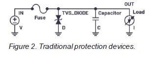
Let us take a closer look at each of these devices, touching on the advantages and disadvantages of this implementation.
TVS—Transient Voltage Suppressor
This is a relatively simple device that helps to protect downstream circuitry from high voltage spikes on the power supply. It can be broken into several different types, which have a wide range of characteristics (Table 1 is in order of response time, smallest to largest).

Although these feature a range of constructions and characteristics, they all operate in a similar manner: shunting the excess current when the voltage exceeds the device threshold. A TVS clamps the voltage at the output to the rated level within a very short period of time. A TVS diode, for example, can respond in as low as picoseconds’ time, while a GDT can take a few microseconds to respond but can handle much larger surges.
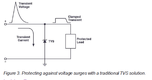
Figure 3 shows the simple implementation of a TVS diode to protect a downstream circuit. Under normal operating conditions, the TVS is high impedance and the input voltage simply passes to the output. When an overvoltage condition occurs at the input, the TVS becomes conductive and responds by shunting the excess energy to ground (GND), clamping the voltage seen by the downstream load. The rail voltage rises above the typical operation value but is clamped to a value at a safe level for any downstream circuitry.
Although TVS devices are effective in suppressing very high voltage excursions, they are not immune to damage when faced with sustained overvoltage events, resulting in a requirement for regular device monitoring or replacement. Another concern is that a TVS can fail short and thus crowbar the input supply. Also, depending on the energy involved, they can be physically large to match with margin, increasing the solution size. Even when a TVS has been correctly sized, the downstream circuitry must be capable of handling the clamped voltage, resulting in increased voltage rating requirements downstream.
In-Line Fuse
Overcurrent protection can be implemented using the ubiquitous in-line fuse with a fuse blow rating at some margin above nominal—for example, 20% higher than the max rated current (the percentage will depend on the type of circuit as well as the typical operational loads expected). The biggest problem with fuses, of course, is that they must be replaced once blown. Time and cost savings resulting from fuses’ simple design can be incurred later because of relatively complex maintenance, especially if the application is physically hard to reach. Maintenance requirements can be reduced with alternate fuses, such as resettable fuses, which utilize a positive temperature coefficient to open the circuit when a larger than normal current passes through the device (the increased current level increases the temperature, resulting in a sharp increase in resistance).
Maintenance issues aside, one of the biggest problems with fuses is their reaction time, which can vary widely depending on the type of fuse selected. Fast blow fuses are available, but clearing time (time to open the circuit) can still range from hundreds of microseconds to milliseconds, so the circuit designer must consider the energy released over these extended times to ensure that downstream electronics can survive.
Series Diode
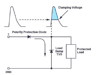
In some environments, circuits are exposed to supply disconnection and reconnection—for example, in a battery-operated environment. In such instances, correct polarity is not guaranteed in reconnection of the supply. Polarity protection can be achieved by adding a series diode on the positive supply line of the circuit. While this simple addition is effective in protecting against reverse polarity, the voltage drop of the series diode results in commensurate power dissipation. In relatively low current circuits, the trade-off is minimal, but for many modern high current rails, an alternative solution is required. Figure 4 shows an update to Figure 3, showing both the TVS and the added series diode to protect against the reverse polarity connection.
Filters Using Inductors and Capacitors
The passive solutions discussed so far all limit the amplitude of the events passed through but generally capture larger events while leaving some smaller spikes to pass. These smaller transients can still cause damage to downstream circuitry, so additional passive filters are required to clean the line. This is achievable using discrete inductors and capacitors, which must be sized to attenuate the voltage at the unwanted frequencies. Filter design requires test and measurement before design to ascertain the size and frequency before the filter can be correctly sized. The drawbacks of this path are the cost of BOM and real estate requirements—the board area and cost of the components required to achieve the level of filtering—as well as the need for overdesign—rating the component tolerances to compensate for changes over time and temperature.
Active Protection Using a Surge Stopper
One way to overcome the challenges and disadvantages of the passive protection solutions described is to instead utilize a surge stopper IC. A surge stopper eliminates the need for bulky shunt circuitry (TVS devices, fuses, inductors, and capacitors) with an easy to use controller IC and a series N-channel MOSFET. Surge stopper controllers can greatly simplify system design since there are few components to size and qualify.
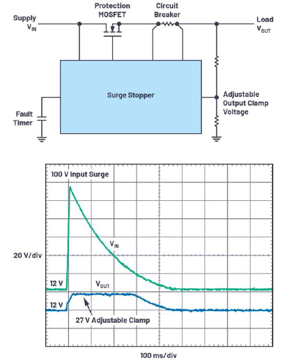
A surge stopper continuously monitors the input voltage and current. Under nominal operating conditions, the controller drives the gate of an N-channel MOSFET pass device fully on, providing a low resistance path from the input to the output. When an overvoltage or surge condition occurs—with a threshold dictated by a feedback network at the output—the IC regulates the gate of the N-channel MOSFET to clamp the output voltage of the MOSFET at the level set by the resistor divider.
Figure 5 shows a simplified schematic of a surge stopper implementation, along with the results of a 100 V input surge on a nominal 12 V rail. The output of the surge stopper circuit is clamped to 27 V for the duration of the surge event. Some surge stoppers also monitor for overcurrent conditions using a series sense resistor (the circuit breaker in Figure 5), and adjust the gate of the N-channel MOSFET to limit the current presented to the output load.
There are four broad types of surge stopper, classified by their response to an overvoltage event:
- Linear surge stopper
- Gate clamp
- Switching surge stopper
- Output disconnect protection controller
The choice of surge stopper depends on the application, so let’s compare their operation and advantages.
Surge Stopper Type: Linear
A linear surge stopper drives the series MOSFET much like a linear regulator would, limiting the output voltage to the pre-programmed safe value, dissipating excess energy in the MOSFET. To help protect the MOSFET, the device limits the time spent in the high dissipation region by implementing a capacitive fault timer.
Surge Stopper Type: Gate Clamp
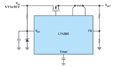
The gate clamp surge stopper operates by utilizing either an internal or external clamp (31.5 V or 50 V internal, for example, or an adjustable external clamp) to limit the gate pin to this voltage. The threshold voltage of the MOSFET then determines the output voltage limit. For example, with an internal 31.5 V gate clamp and a MOSFET threshold voltage of 5 V, the output voltage is limited to 26.5 V. Alternately, an external gate clamp allows a much wider range of voltages to be selected. An example of a gate clamp surge stopper is shown in Figure 7.
Surge Stopper Type: Switching
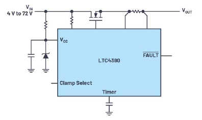
For higher power applications, a switching surge stopper is a good choice. Like linear and gate clamp surge stoppers, a switching surge stopper fully enhances the pass FET under normal operation to provide a low resistance path between the input and output (minimizing power dissipation). The main difference between a switching surge stopper and a linear or gate clamp surge stopper appears when a surge event is detected. In the event of a surge, the output of a switching surge stopper is regulated to the clamp voltage by switching the external MOSFET much like a switching dc-to-dc converter.
Protection Controller: Output Disconnect
A protection controller is not officially a surge stopper, but it does stop surges. Like a surge stopper, a protection controller monitors for overvoltage and overcurrent conditions, but instead of clamping or regulating the output, the protection controller disconnects the output immediately to protect downstream electronics. This simple protection circuit can have a very compact footprint, suitable for battery-operated, portable applications. The LTC4368 protection controller is shown in a simplified schematic in Figure 9, along with its response to an overvoltage event. Protection controllers are available in a number of variants.
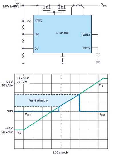
A protection controller operates by monitoring the input voltage to ensure that it remains within a voltage window configured by the resistor divider on the OV/UV pins, disconnecting the output via back-to-back MOSFETs when the input is outside this window, as shown in Figure 9. The back-to-back MOSFETs can also protect against a reversed input. The sense resistor at the output enables overcurrent protection capability by continually monitoring the forward current, but without a timer-based ride-through operation.
Surge Stopper Features
In order to select the most suitable surge stopper for your application you will need to know what features are available and what challenge they are helping to solve. The devices can be found at the parametric table.
Disconnect vs. Ride-Through
Some applications require disconnecting the output from the input when a surge event is detected. In this instance, overvoltage disconnect would be required. If you needed the output to remain operational in the face of surge events, thus minimizing the downtime of downstream electronics, you would require the surge stopper to ride through the surge event. In this case, a linear or a switching surge stopper can achieve this functionality (provided the power levels were reasonable for the topology and FET selected).
Fault Timer
Ride-through operation requires some protection for the MOSFET against persistent surges. To remain within the safe operating area (SOA) of the FET, a timer can be implemented. The timer is essentially a capacitor to ground. When an overvoltage condition occurs, an internal current source starts to charge this external capacitor. Once the capacitor reaches a certain threshold voltage, a digital fault pin pulls low to indicate the pass transistor will soon turn off due to the extended overvoltage condition. If the timer pin voltage continues to rise to a secondary threshold, the GATE pin pulls low to turn off the MOSFET.
The rate of change of the timer voltage varies with the voltage across the MOSFET—that is, a shorter timer for larger voltages and a longer timer for smaller voltages. This useful feature enables the device to ride through short overvoltage events, allowing downstream components to remain operational while protecting the MOSFET from damage by longer-lasting overvoltage events. Some devices feature a retry function, enabling the device to turn on the output again after a cool down period.
Overcurrent Protection
Many surge stoppers have the ability to monitor current and protect against overcurrent events. This is achieved by monitoring the voltage drop across a series sense resistor and responding appropriately. Inrush current can also be monitored and controlled to protect the MOSFET. The response can be similar to an overvoltage condition, as it either disconnects by latching off or riding through the event if the circuitry can handle the power levels.
Reverse Input Protection
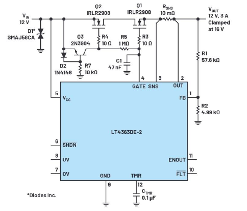
Reverse input protection is possible due to the wide operating capabilities of the surge stopper devices (capable of withstanding up to 60 V below ground potential on some devices). Figure 10 shows a back-to-back MOSFET implementation of reverse current protection. During normal operation, Q2 and Q1 are turned on by the GATE pin, and Q3 doesn’t have any impact. However, when a reverse voltage condition exists, Q3 turns on, pulling Q2’s gate down to the negative input and isolating Q1, protecting the output.
Reverse output voltage protection is also achieved with robust device pin protection, with up to 20 V below ground potential possible, depending on the device selected.
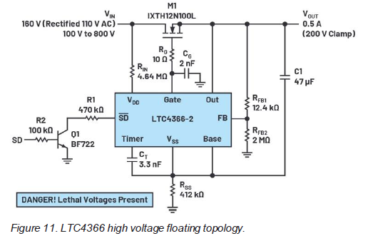
For applications that require wide input voltage ranges, a floating topology surge stopper can be used. When a surge event occurs, the full surge voltage is seen by the surge stopper IC so the internal transistor technology limits the voltage range of the IC. With a floating surge stopper such as the LTC4366, the IC floats just below the output voltage, giving it a much wider operating voltage range. A resistor is placed in the return line (VSS), which allows the IC to float up with the supply voltage. The result is an input voltage limitation set by the voltage capability of the external components and MOSFETs. Figure 11 shows an application circuit capable of operating from a very high dc supply while protecting the downstream load.
Choosing the Right Device for My Application
In many ways, because of their inherently robust design, using a surge stopper simplifies protection circuit design. Data sheets can help greatly with sizing components, with many possible applications already shown. The hardest part might be choosing the most appropriate device. Follow these few steps to narrow the field:
- Go to ADI’s protection family parametric table.
- Choose input voltage range.
- Choose the number of channels.
- Filter on features to narrow the possible options.
As with all product selection, it is important to understand your system requirements before looking for the correct device. Some important considerations are the expected supply voltage and the voltage tolerance of downstream electronics (important for deciding the clamp voltage), as well as any particular features that are important for the design.
Some example filtered parametric tables are shown below for reference. These can further be modified on the website to include some other parameters.
- The high voltage surge stopper devices can be found here.
- Protection controllers with the OV disconnect feature can be found here.
Conclusion
Regardless of the surge stopper type implemented, active, IC-based surge stopper designs eliminate the need for bulky TVS diodes or large profile inductors and capacitors for filtering. This results in an overall smaller area and a lower profile solution. The output voltage clamp is more accurate than a TVS with 1% to 2% accuracy possible. This prevents overdesign and allows for downstream devices with tighter tolerances to be selected.
The system protection family of devices available from Analog Devices enables designers to implement reliable, flexible, and small form factor protection for downstream devices—especially those facing harsh overvoltage and overcurrent events, which can occur in many industrial-, automotive-, aerospace-, and communications-based designs.
References
“AN-9768: Transient Suppression Devices and Principles.” Littelfuse, January 1998.
“Fuseology.” Automotive Passenger Car Solutions Catalog, Littelfuse, 2014.
Kalb, Jim. “Total Cleari ng Time” Technical Bulletin, OptiFuse, January 2010.
Megaw, David. “Protecting and Powering Automotive Electronics Systems with No Switching Noise and 99.9% Efficiency.” Analog Dialogue, Vol. 54, No. 1, February 2020.
Wu, Bin and Zhongming Ye. “Comprehensive Power Supply System Designs for Harsh Automotive Environments Consume Minimal Space, Preserve Battery Charge, Feature Low EMI.” Analog Dialogue, Vol. 53, No. 3, August 2019.
Author
Diarmuid Carey
Diarmuid Carey is an applications engineer with the European Centralized Applications Center based in Limerick, Ireland. He has worked as an applications engineer since 2008 and joined Analog Devices in 2017, providing design support for the Power by Linear portfolio for European broad market customers. He holds a Bachelor of Engineering in computer engineering from University of Limerick.


