By Vaishali Umredkar
 EDA industry is dependent on the growth of semiconductor industry. Innovation in semiconductor design and manufacturing, such as lithography, material science and package design, is leading to high-performance, miniaturized, energy-efficient devices — powering the smart product revolution. At each semiconductor process node, engineers are challenged by the physics associated with shrinking geometries. Complexity of the geometries involved will have a dramatic impact on every aspect of the EDA tool chain. Therefore, an ever closer interaction between these tools is needed to ensure that the overall product goals can be met.
Contributors Profile
 This year onwards we shall see increased connectivity of the electronic devices that are pervasive in our world today. This trend will continue to drive the existing mobile market growth as well as make an impact on upcoming automotive electronics.
As per Gartner report, by 2017, the semiconductor industry will be facing a future where Moore’s Law is no longer the primary driving force for industry growth. Innovation will shift from wafer manufacturing to a broad range of options, including software and packaging, as industry focus shifts to the Internet of Things.
Jaswinder Ahuja, Corporate Vice President and the Managing Director of Cadence Design Systems in India quotes on electronics opportunities in India, “This is a very exciting time for the electronics and semiconductor industries. Traditional product categories like entertainment, computing, and even automotive are seeing a stream of new features and innovations, and even more exciting are the completely new product categories like wearable electronics and personal health devices that will drive innovation and growth in the electronics business”.
It’s a big challenge for semiconductor companies to remain competitive in these markets, they will need to take a “system” view for their design and verification. The traditional silo-based methodology, where each component of the system is designed and analyzed independently can result in products with higher cost, poor quality, and schedule delay. An adoption of system-level simulation will allow engineers to carry out early system prototyping, analyze the interaction of each of the components, and achieve optimal design tradeoffs.
The EDA industry tracks the trends in the semiconductor industry which is constantly evolving to cater to the 130, 90, 65 and even 45-nm silicon geometries. The whole electronics industry depends on the efficiency of these EDA tools, which would ensure smaller, faster, cheaper and more intelligent next-generation electronic products.
The EDA tools industry faces a high degree of technical change as it follows the technologically advanced semiconductor industry. The EDA tool vendors need to meet the design requirements of the semiconductor industry. The continuous size reduction in ICs from micro- to nanoscale dimensions drives the need for advanced and innovative EDA technologies to design the ever-shrinking devices.
“EDA industry has been fairly stable with growth in the 5-7% range for a few years now. Within the SoC Realization space and above, we believe there is an opportunity for significant growth. In this area of EDA, there will continue to be new companies and new ideas emerging to address future challenges”, says Sushil Gupta, Vice President and Managing Director, Atrenta India. He adds, “The two trends we see are focused on addressing the challenges of complexity. The substantial rise in design complexity is making signoff at RTL more and more important. Without it, significant iterations are seen during implementation which causes rework and significant delays. The complexity is also driving the need for more and more reuse of IP blocks. This is because you can no longer be an expert in all of the functions of the design. Nor do you have the time to develop all of these functions on your own. This makes IP selection and qualification critically important to ensure that the building blocks of your design are solid and integrated well with the other pieces.”
Arun Mulpur, WW Industry Manager, MathWorks India comments, “It is not surprising that innovation and integration in a variety of fields – from semiconductors to automotive electronics to medical devices – is the biggest opportunity and the primary growth driver for EDA. At a high level, in most high-tech industries and applications, innovation drives growth, and in turn, innovation is driven by engineering efficiencies. EDA industry itself is innovating to in order to support the innovation in these fields.
Automatic Verilog and VHDL code generation from algorithm designs and system models, automatic test bench generation, and integration of models with other EDA synthesis and verification flows are some of the key EDA innovations from the past few years. In the near future, this trend will continue with better integration of Model-Based Design workflows for digital, analog, and mixed-signal designs”.
He mentions key focus of EDA Industry as, “IP libraries, virtual prototyping, high level synthesis, and support of new semiconductor design nodes such as 14nm are some of the issues that the EDA industry has been focusing on in the recent past”.
EDA industry is very competitive and is more technology driven. As the design complexities increase, designers demand more innovative and complex tools and as the time to market pressures are increasing, EDA companies are always under great pressure to roll out sophisticated tools to understand and solve design complexities. Having said this, it can be easily understood that EDA industry works in tight integration with the Design companies and the manufacturers. Each chip is designed in a different way and the Methodology engineers propose new Methodologies and flows which indirectly puts pressure on the EDA industry. Atrenta is addressing well all these issues.
Sushil Gupta of Atrenta India pointed, “The current challenges in EDA are related to the growing demands of the consumers for smarter and more efficient electronic devices. The design complexity has increased substantially with companies designing SoCs based on semiconductor processes of 28nm and below. The cost of developing an SoC at these geometries is in tens of millions dollars.
The mobile revolution has created serious demand for low power consumption while maintaining functionality and performance. Firms creating IP for applications such as phones, tablets, cameras, and various types of wireless applications such as Bluetooth, wi-fi and the like, are concerned about power, while those who are creating wired applications are more concerned about performance.
Additionally, anything linked to the consumer industry has an increasing time to market pressure because the consumer market is very cyclic and expects new additions of technology every 6 months or so. EDA plays an important role here in providing enabling technologies and infrastructure to help put the IPs together and create an SoC that meets the time to market, power, performance and cost requirements of the application”.
“Verification continues to be a major challenge because it grows at a faster pace than the design challenges.” Sushil adds. He further elaborates, “This makes it critical to begin the verification as early as possible, when it is easier to find and correct problems. Our RTL Signoff campaign has resonated very well over the past year and our partners are seeing great productivity gains as a result.
At the RTL, our partners can analyze their design for many critical problem areas including power, DFT (design for test), constraints, CDC (clock domain crossing), physical congestion, and functional verification closure. By doing so, upfront in the RTL, they can avoid costly iterations with expensive tools downstream and reduce their schedules by as much as 60%. This is often the difference in a successful product launch and failure”.
According to Arun Mulpur, WW Industry Manager, MathWorks India, “Many of the semiconductor and electronics industry leaders that I have spoken to recently mentioned that the primary issues facing their organizations are in improving RTL to layout; System Design and Virtual Prototyping; and Top-Down Design of Mixed-Signal SoCs. The EDA industry would do well to heed this call to action from their customers.”
He adds, “System Design / Virtual Prototyping, and Top-Down Design of Mixed-Signal SoCs are some of the key issues facing the EDA customer community. Verification at all levels – from initial behavioral and functional verification all the way to final sign-off verification – continues to be the biggest expense and the largest latency in EDA. The majority of the EDA industry initiatives to address the verification challenges have been disjointed and half-hearted attempts for the simple reason that they have been mostly bottom-up approaches.To fundamentally change the verification equation, the EDA industry must truly and fully embrace Model-Based Design”.
IP business model
Everyone today understands the essential importance of third-party semiconductor intellectual property (IP) to the health of the semiconductor industry. Considerably less attention is given to the importance of a strong, serviceable portfolio of internal IP within a semiconductor company.
Since the beginning of the semiconductor industry, chip companies have had strong, thriving portfolios of IP that differentiated them from their competitors. Until the mid-1980’s, these companies were “vertically integrated” with their own foundries, EDA tools, and IP. That all changed in the 1980’s when TSMC came into the picture and began an era of disaggregation. No longer did a company need to have its own expensive foundry for producing chips. The same happened with EDA, where legions of companies such as Synopsys, Mentor, and Cadence came onto the scene to increase efficiencies even further. Companies could then focus on their true competency—design.
The final step of disaggregation began in the 1990’s, when third-party IP companies like ARM and Artisan appeared on the market to allow new semiconductor companies to form and build thriving businesses using third-party foundries, EDA, and now IP. These new-breed semiconductor companies (aka “fabless”) continued to differentiate themselves with their own “special sauce”—internal IP coupled with commodity, off-the-shelf IP, assembled in unique ways. Today, the most advanced chip companies closely guard their special sauce recipes by investing significantly in internal IP efforts to stay ahead of their competitors.
The semiconductor Intellectual Property (IP) market is expanding rapidly in size and prominence at a growth rate which is two times faster than the overall semiconductor market. As process technologies shrink further in the sub-nanometer level, the gap between accessible silicon and designers’ ability to utilize that space keeps widening.
IP is vital in ameliorating design productivity at advanced design processes. With relatively slower growth in the overall semiconductor market, expense management has gained focus, which is driving the growth of third-party IP vendors. Semiconductor players are actively outsourcing the IP design and development activities not core to their product differentiation. The growing trend of third-party IP Vendors and increasing licensing of advanced IP blocks by several key players are bound to change the landscape of the global semiconductor IP market.
For many years IP licensing has been a fragmented industry comprising myriad small, independent suppliers. However, large EDA vendors are aggressively pursuing the business opportunity, acquiring numerous companies to accelerate their entry. EDA companies’ aggressive pursuit of the IP business is a boon for semiconductor companies, and it enables integrated Device manufacturers and fables suppliers to focus their R&D sources on creating more value added IP. On the other hand, as the breadth and depth of their IP portfolios expand, EDA vendors themselves become supplier of added value, which ones belonged to semiconductor companies. During this transition, EDA vendors invariably become competitors of the chip companies’ internal R&D organization, much as they did 20 years ago when they displaced the internal computer-aided-design groups of semiconductor companies.
“The IP market opportunity is quite extensive. The key to success is providing high quality IP that is easy to integrate into an SoC with confidence”, says Sushil. “The Atrenta IP Kit is the standard which over 20 companies have adopted, including TSMC, to ensure that they have passed the approved, standard IP quality checks. The IP Kit also provides standard documentation to their customers about the testing and qualification they have done, and configurations they support, to ensure a smooth integration into their SoC design”, he adds.
“Most IP designs begin in MATLAB”, says Arun Mulpur, WW Industry Manager, MathWorks India. “As a result, many EDA insiders agree that MATLAB is by far the most important EDA design tool in the world today. Together, MATLAB and Simulink –along with DSP System Toolbox, Communications System Toolbox, and Computer Vision System Toolbox – provide a complete and proven platform for algorithm development and system design. In addition, MathWorks continues to work with leading semiconductor companies worldwide to customize solutions for integrated EDA flows for digital and mixed-signal system design, implementation, and verification through innovative application of its C code generation (Simulink Coder, Embedded Coder) and circuit m o d e l i n g ( S i m s c a p e , S i m E l e c t r o n i c s , SimPowerSystems) technologies, and integration with leading third-party EDA synthesis and simulation platforms”, adds Arun.
Shared Approach
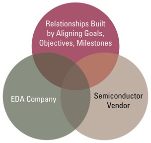
Over the last 10 years, electronic design automation (EDA) companies have tried various methods to partner with new ventures, but not without re-occurring fundamental challenges. New ventures, by their nature, are exciting and cutting-edge, but limited in tool volume and revenue. A variety of approaches have been taken, including investments and lower venture pricing (perhaps also with reduced support). Remember the pre-telecom days? But at the end of the day, EDA companies are not venture capitalists, and after a few failed attempts, the sector has returned to square one.

Fabless and, often, small semiconductor companies need EDA’s support and technology access. As EDA moves slowly out of the latest catastrophic meltdown, it’s more important than ever to consider that fabless semiconductor ventures and EDA companies have a shared destiny and must find new ways to partner.
One of the most difficult and critical core technology decisions a fabless company must make is whether to develop or source IP. Many large EDA companies are building IP portfolios that new ventures may find useful, but these ventures may not have the resources available to buy the IP. Alternatively, some companies will license IP for the duration of the project, while other more creative firms will allow a start-up to mix in and out certain pieces of IP over the project’s lifetime under the same license.
Another difficult task is building a world-class development team that is increasingly globalized. Multi-core system-on-chip (SoC) design and its complexity drive fabless ventures to quickly scale software and hardware teams. External development partners can play a role, particularly in enabling technology. Software frequently falls into this category.
What the EDA Wants
Often, an EDA vendor can relate to these challenges and, with some creativity, help a fabless start-up address them. Many EDA players have spent time with fabless start-ups and have enjoyed working with them. But most secretly hope that these companies will either become big fast or merge with a large customer, carrying praises of their EDA supplier’s technology with them. And it is hoped that special business models, if provided, will be balanced by lower support costs.
As new fabless ventures look at EDA and EDA looks at new fabless ventures, there may be other synergies identified that both are missing, and values both can gain in the short term and long term by working together.


