With No Switching Noise and 99.9% Efficiency
By David Megaw, Senior Design Engineer, Analog Devices

Powering automotive electronics systems can be challenging due to requirements of high reliability while contending with a relatively unstable battery voltage. The variety of electrical and mechanical systems that interface with a vehicle’s battery can cause wild voltage excursions in the nominal 12 V supply. In reality, 12 V can vary from –14 V to +35 V for extended periods of time and experience voltage spikes with extremes ranging from +150 V to –220 V. Some of these surges and transients arise from everyday use, others from fault conditions or human error. Regardless of cause, the damage they can produce in a vehicle’s electronics system can be difficult to diagnose and expensive to fix.
The experience of automakers over the last century has led to a catalog of electrical conditions and transients that are known to disrupt operation and cause damage. The International Organization for Standardization (ISO) has compiled this industry knowledge into the ISO 16750-2 and ISO 7637-2 specifications for road vehicles. At a minimum, the power supply for an automotive electronic control unit (ECU) should survive these conditions without damage. For critical systems, functionality and tolerances must be maintained. This requires that the power supply regulates the output voltage through the transient to preserve ECU operation. Ideally, a complete power solution avoids the need for fuses, minimizes power dissipation, and features low quiescent current to support always-on systems without draining the battery.
ISO 16750-2 Conditions for Automotive Electronics Systems
Analog Devices has several publications covering the ISO 7637-2 and ISO 16750-2 specifications in detail, along with how to simulate them using LTspice®.
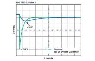
In its latest iteration, the ISO 7637-2 electromagnetic compatibility specification focuses on high amplitude (>100 V), short duration (150 ns to 2 ms) transients from relatively high impedance sources (2 Ω to 50 Ω). These voltage spikes can often be mitigated with passive components. Figure 1 shows ISO 7637-2 pulse 1 as defined and with an added 330 µF bypass capacitor. The capacitance reduces the spike’s amplitude from –150 V to –16 V, well within the range of reverse battery protection circuitry. ISO 7367-2 pulses 2a, 3a, and 3b have significantly lower energy than pulse 1 and require less capacitance to suppress.
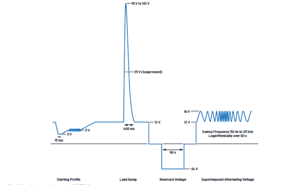
ISO 16750-2 focuses on longer duration pulses from low impedance sources. These transients cannot easily be filtered and frequently require active, regulator-based solutions. Some of the more challenging tests include the load dump (test 4.6.4), the reverse battery condition (test 4.7), the superimposed alternating voltage test (test 4.4), and the engine starting profile (test 4.6.3). Figure 2 gives a visual overview of these test pulses. The variety of conditions presented in ISO 16750-2, along with the voltage and current requirements of the ECU, frequently require a combination of approaches in order to satisfy them all.
Load Dump
A load dump (ISO 16750-2: test 4.6.4) is a severe overvoltage transient that models a battery disconnect while the alternator is sourcing substantial current. The peak voltage during a load dump is classified as either suppressed or unsuppressed, depending on whether avalanche diodes are used on the outputs of the 3-phase alternator. A suppressed load dump pulse is limited to 35 V, whereas an unsuppressed pulse peak ranges from 79 V to 101 V. In either case, it can take up to 400 ms to recover due to the large amount of magnetic energy stored in the alternator’s stator windings. While most automakers utilize avalanche diodes, increasing reliability demands are driving some manufacturers to require that ECUs satisfy peak load dump voltages approaching that of the unsuppressed case.
One solution for facing load dumps is adding a transient voltage suppressor (TVS) diode to locally clamp the ECU supply. A more compact and tighter tolerance approach is to use an active surge stopper, such as the LTC4364, which linearly controls a series N-channel MOSFET to clamp the maximum output voltage to a user-programmed level (for example, 27 V). Surge stoppers add the ability to disconnect the output, allowing programmable current limit and undervoltage lockout, and often provide reverse battery protection when back-to-back NFETs are used.
The concern with any linearly regulated power device such as a surge stopper is the potential for significant power dissipation in the N-channel MOSFET(s) when limiting the output voltage during a load dump, or when limiting current with a shorted output. The safe operating area (SOA) constraints of the power MOSFET ultimately limit the maximum current possible with a surge stopper. It also puts a time limit (typically set with a programmable timer pin) on how long regulation can be maintained before the N-channel MOSFET must be shut off to avoid damage. These SOA imposed limitations become more acute at higher operating voltages, making surge stopper use trickier for 24 V and 48 V systems.
A more scalable approach is to use a buck regulator capable of operating with a 42 V input, such as the LT8640S. A switching regulator doesn’t have the MOSFET SOA limitations of a linear regulator, but it is certainly more complex. The efficiency of a buck regulator allows for very high current operation, and its top switch permits output disconnect and current limiting. Concerns about buck regulator quiescent current have been put to rest with the latest generation of parts that draw only a few microamps while in regulation under no load conditions. Switching noise has also improved substantially with Silent Switcher® technology and spread spectrum frequency modulation techniques.
Additionally, some buck regulators are able to operate at 100% duty cycle such that the top switch is on continuously, passing the input voltage to the output through the inductor. Switching operation is triggered during overvoltage or overcurrent conditions to limit output voltage or current, respectively. These buck regulators, such as the LTC7862, act as switching surge stoppers, achieving low noise, low loss operation while still retaining the robustness of a switch-mode power supply.
Reverse Voltage
A reverse voltage condition (also known as a reverse battery condition) occurs when battery terminals or jumper cables are connected backward due to operator error. The relevant ISO 16750-2 pulse (test 4.7) applies –14 V to the DUT for 60 second durations, repeatedly. Some manufacturers add their own dynamic versions of this test where the part is initially powered (for example, VIN = 10.8 V) before a reverse bias (–4 V) is abruptly applied.
A quick survey of data sheets shows that few ICs are designed to tolerate negative biases, with IC absolute minimum pin voltages typically limited to –0.3 V. Voltages more than a diode below ground can cause excessive current flow through internal junctions such as ESD protection devices as well as body diodes of power MOSFETs. Polarized bypass capacitors such as aluminum electrolytics may also be damaged during the reverse battery condition.
A Schottky diode can prevent reverse currents, but this approach leads to significant power loss at higher forward currents in normal operation. A simple protection scheme based on series P-channel MOSFET shown in Figure 3 reduces this loss, but may not work well at low input voltages (for example, engine start) due to the device threshold voltage. A more efficient approach is to use an ideal diode controller, such as the LTC4376, which drives a series N-channel MOSFET that cuts off input voltages below ground. In normal operation, an ideal diode controller regulates the source to drain the voltage of the N-channel MOSFET to 30 mV or less, reducing forward voltage drop and power dissipation by more than an order of magnitude compared to a Schottky diode.
Superimposed Alternating Voltage
The superimposed alternating voltage test (ISO 16750-2: test 4.4) models the impact of the ac output of the vehicle’s alternator. As the name implies, a sinusoidal signal is superimposed on the battery rail with peak-to-peak amplitude of 1 V, 2 V, or 4 V, depending on severity level classification. For all severity levels, the maximum input voltage is 16 V. The frequency of the sinusoid is swept logarithmically from 50 Hz to 25 kHz and then back to 50 Hz over 120 seconds and repeated a total of five times. This test causes large amplitude current and voltage swings in any connected filter network with a resonance below 25 kHz. It can also cause problems for switching regulators where loop bandwidth limitations make it a struggle to regulate through high frequency input signals. One solution is an intermediate rectifying element such as a power Schottky diode, but as with reverse voltage protection, this is a poor way to solve the problem.
An ideal diode controller will not work here like it did for reverse voltage protection because it cannot switch the N-channel MOSFET sufficiently fast to keep up with the input. The limiting factor is the gate pull-up strength, which is typically limited to 20 µA or so by an internal charge pump. While the ideal diode controller can quickly turn the MOSFET off, turn on is painfully slow, unsuitable for rectification of anything beyond very low frequencies.
A more elegant approach is to use the LT8672 active rectifier controller, which can toggle an N-channel MOSFET fast enough to rectify the input voltage at frequencies up to 100 kHz. An active rectifier controller is an ideal diode controller with two important additions: a large reservoir of charge boosted up from the input voltage and a powerful gate driver to toggle the N-channel MOSFET both on and off quickly. This method can reduce power loss by more than 90% compared to a Schottky. The LT8672 also protects downstream circuitry from a reverse battery condition just as an ideal diode controller would.
Starting Profile
The engine starting profile (ISO 16750-2: test 4.6.3) is an extreme undervoltage transient, sometimes referred to as the cold crank pulse because the worst-case battery droop occurs at lower temperatures. Specifically, when the starter turns over, the 12 V battery voltage can momentarily drop to 8 V, 6 V, 4.5 V, or 3 V, depending on severity level classification (I, IV, II, III, respectively).
In some systems, a low dropout (LDO) linear regulator or switching buck regulator is sufficient to allow power rails to ride through this transient, provided that ECU voltages are less than the lowest input voltage. For example, if the highest ECU output voltage is 5 V, and it must satisfy severity level IV (minimum input voltage of 6 V), then a regulator with a dropout voltage less than 1 V is enough. The lowest voltage segment of an engine starting profile lasts for only 15 ms to 20 ms, so a rectifying element (Schottky diode, ideal diode controller, active rectifier controller) followed by a large bypass capacitor may be able to ride through this portion of the pulse if the voltage headroom briefly dips below the regulator dropout.
If, however, the ECU must support voltages higher than the lowest input voltage, then a boost regulator is required. Boost regulators can efficiently maintain a 12 V output voltage from inputs less than 3 V at high current levels. There is one problem with a boost regulator, though: the diode path from input to output prevents disconnect, so current is not naturally limited at startup or due to a short. To prevent current runaway, specialized boost regulators, such as the LTC3897 controller, incorporate a surge-stopper front end to allow output disconnect and current limiting, as well as provide reverse voltage protection when back-to-back N-channel MOSFETs are used. This solution can address the load dump, engine start, and reverse battery conditions with a single integrated circuit, but available current is limited by the SOA of the surge-stopper MOSFET.
A 4-switch buck-boost regulator lifts this constraint by combining a synchronous buck regulator and a synchronous boost regulator through a shared inductor. This approach can satisfy both the load dump and engine starting profile tests without MOSFET SOA limitations on current level or pulse duration, while retaining the ability to disconnect the output and limit current.
The switching operation of a buck-boost regulator depends on the relationship between the input and output voltages. If the input is significantly higher than the output, the boost top switch turns on continuously while the buck power stage steps down the input. Similarly, when the input is significantly lower than the output, the buck top switch turns on continuously while the boost power stage steps up the output. When the input and output are roughly equal (within 10% to 25%), the buck and boost power stages switch simultaneously in an interleaved fashion. In this way, efficiency is maximized in the various switching regions (buck, buck-boost, boost) by limiting switching to only the MOSFETs required for regulation for input voltages above, roughly equal to, or below the output, respectively.
ISO 16750-2 Solution Summary
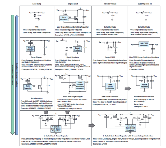
Figure 3 summarizes the various solutions to addressing the load dump, reverse input voltage, superimposed alternating voltage, and engine starting profile tests along with the pros and cons of each approach. Several key take-a ways begin to emerge:
• A series N-channel MOSFET with its drain facing the input is extremely desirable because it can be used to limit current and disconnect the output whether it’s used as a switch (for example, in a buck power stage) or linearly controlled (for example, in a surge stopper).
• In the case of reverse input protection and superimposed alternating voltage, using an N-channel MOSFET as the rectifying element (source facing the input) significantly reduces power loss and voltage drop compared to a Schottky diode.
• A switch-mode power supply is preferable to a linear regulator because it alleviates the reliability concerns and output current restrictions that come with operating within the SOA of the power device. It can regulate at input voltage extremes indefinitely, whereas linear regulator and passive solutions have inherent time limitations that complicate design.
A boost regulator may or may not be necessary depending on the severity classification of the starting profile and the details of the ECU (what’s the highest voltage it must provide).
If boost regulation is called for, then a 4-switch buck-boost regulator combines the above desirable traits into a single part. It can efficiently regulate through severe undervoltage and overvoltage transients at high current levels for extended periods of time. This makes it the most robust and straightforward approach, from an applications standpoint, despite the increased design complexity. Nevertheless, a typical 4-switch buck-boost regulator has some drawbacks. For one, reverse battery protection is not naturally provided and must be addressed with additional circuitry.
The primary shortcoming of the 4-switch buck-boost regulator is that it spends much of its operational life in the lower efficiency, noisier buck-boost switching region. When the input voltage is nearly equal to the output (VIN ~ VOUT) all four N-channel MOSFETs are actively switching to maintain regulation. Efficiency drops as a result of increased switching losses and application of maximum gate drive current. Radiated and conducted EMI performance suffer in this region as both the buck and boost power-stage hot loops are active and the regulator input and output currents are discontinuous.
A 4-switch buck-boost regulator can regulate through occasional large amplitude undervoltage and overvoltage transients, but at the price of operating with high quiescent current, lower efficiency, and increased noise in the far more common, nominal conversion region.
Pass-Thru Operating Mode Brings High Efficiency and EMI Performance Buck-Boost Region
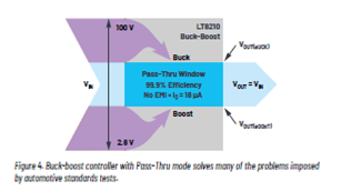
The LT8210 is a 4-switch buck-boost dc-to-dc controller that can operate conventionally with a fixed output voltage and also features a new Pass-ThruTM operating mode (Figure 4), which eliminates the switching losses and EMI through a programmable input voltage window. It operates from 2.8 V to 100 V, allowing it to regulate through the most severe battery drop during engine start to the peak amplitude of an unsuppressed load dump. It comes with built-in reverse battery protection to –40 V, which is implemented with the addition of a single N-channel MOSFET (DG in Figure 5).
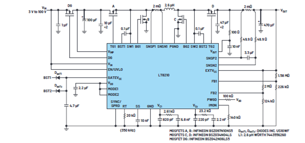
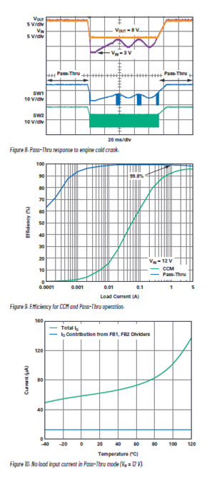
In Pass-Thru mode, the output voltage is regulated to the edges of a voltage window when the input voltage is outside the window. The top of the window and the bottom are programmed via the FB2 and FB1 resistor dividers. When the input voltage is within this window, the top switches (A and D) turn on continuously, passing the input voltage directly to the output. In this nonswitching state, the total LT8210 quiescent current drops to tens of microamps. The absence of switching means no EMI and no switching losses, enabling efficiencies of greater than 99.9%.
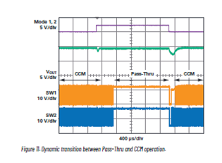
For those who want the best of both worlds, the LT8210 allows transitioning between its different operating modes on-the-fly by toggling the MODE1 and MODE2 pins. In other words, the LT8210 can operate as a conventional buck-boost regulator with fixed output voltage (in CCM, DCM, or Burst Mode™) in some situations and then change to Pass-Thru mode as the conditions in the application change. This can be a useful feature for always-on systems and in start-stop applications.
Pass-Thru Performance
The Pass-Thru solution in Figure 5 passes the input to output in the window between 8 V and 17 V. When the input voltage is above the Pass-Thru window, the LT8210 bucks it down to a regulated 17 V output. If the input drops below 8 V, the LT8210 boosts the output to 8 V. As a protection feature, switching operation is triggered within the Pass-Thru window to control current if either the inductor current limit or programmed average current limit (via the IMON pin) are exceeded.
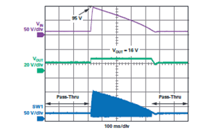
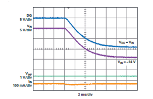
Figure 6, Figure 7, and Figure 8 show the response of the LT8210 circuit to the load dump, reverse voltage, and starting profile tests, respectively. Figure 9 and Figure 10 demonstrate the efficiency improvement and low current operation possible while in the Pass-Thru window (it’s amazing how efficient doing nothing can be). Figure 11 shows the dynamic transition between Pass-Thru mode and CCM operation. An LTspice simulation of this circuit along with sped up versions of the toughest ISO 16750-2 test pulses is available at analog.com/media/en/simulation-models/LTspice-demo-circuits/LT8210_AutomotivePassThru.asc.
Conclusion
When designing a power supply for an automotive electronic system, the LT8210 4-switch buck-boost dc-to-dc controller offers a superior solution with its 2.8 V to 100 V input operating range, built-in reverse battery protection, and its new Pass-Thru operating mode. Pass-Thru mode improves upon buck-boost operation, achieving no switching noise, no switching losses, and ultralow quiescent current while regulating the output to a user-programmed window rather than a fixed voltage. The output voltage minimum and maximum values are bounded during large amplitude transients such as load dump and cold crank without MOSFET SOA concerns, or the current or timing limitations that come from linear solutions.
The novel LT8210 control scheme results in clean and fast transitions between the different switching regions (boost, buck-boost, buck, and nonswitching) allowing it to regulate through large signal, high frequency ac voltage on the input. For more details, please refer to the video at analog.com/en/education/educationlibrary/videos/6136638907001.html. The LT8210 can be toggled between Pass-Thru operation and conventional, fixed output voltage, buck-boost operating modes (CCM, DCM, or Burst Mode) while running, and the fixed output can be set to any voltage within the Pass-Thru window (for example, VOUT = 12 V for an 8 V-to-16 V window). This flexibility allows the user to alternate between Pass-Thru and normal buck-boost operation to trade the low noise, low IQ, high efficiency operation of Pass-Thru mode for the tighter regulation and improved transient response in CCM, DCM, or Burst Mode.


