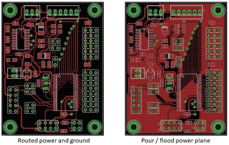
Power distribution on a PC board can come in a number of forms. The three most common methods are:
- You can route power and ground
- You can use surface layer floods
- You can use internal planes
 After component positioning, you’ll need to look at power and ground distribution. With a two layer board, your options are limited to individually routing power and ground, or using a polygon fill, also called a flood or pour.
For simple, low speed layouts, it’s common to route power just like any other signal. You’ll typically use a wider trace, which you can set manually, or with design rules. Drawing a polygon in the board shape, and giving it the same name as your power or ground signals may make the job easier. Keep in mind that you can end up with parts of a ground plane that are disconnected from the rest of the board. This is called an orphan. Some CAD error checks will spot such a problem and some won’t.
If you have a four or more layer board, common practice is to designate one of the internal layers for ground, and one for power. Doing so can leave more room for signal routing, can reduce EMI and can leave a cleaner looking, and easier-to-debug board. It also reduces the chances of having orphan ground or power areas.


