
By Van Yang, FAE, Analog Devices, Inc.
In many applications such as computing, the power rail’s load transient requirement are becoming more and more restrictive. Furthermore, because it involves complex Laplace transfer function calculations, the loop compensation design is often viewed as a difficult and time consuming task for many engineers.
This article discusses, step by step, the average small signal modeling of widely-used peak current mode continuous current mode DC-DC converters. With the mathematical model, ADI’s ADIsimPE/Simplis, a switching circuit’s simulation tool, was introduced to minimize the work of complex calculation. Then offered a simplified model for simpler and faster loop compensation design and simulation. The ADP2386EVAL test results proved that the loop cross over frequency, phase margin and load transient response simulation results were well matched with test results.
PCM average small signal modeling
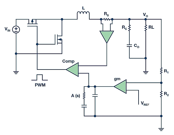
As the Figure 1 shows, six blocks contribute to the current mode DC-DC converter function: the feedback resistor divider, the compensator network, the current sensing and sampling, the comparator, the power stage, and the output network. In the loop, the inductor current ramp signal is compared with the compensator error amplifier output, which feedbacks from output voltage. The PWM signal is generated to drive the switches to modulate inductor current. Inductor current flows into the output capacitor and load. Of these six blocks, the power stage is the only non-linearized block and it can be the most difficult block for DC-DC modeling.
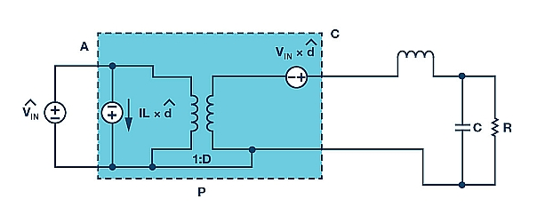
Modeling the power stage as a 3-terminal switch: 1) active switch node (A), 2) common mode (C), and 3) passive switch node (P), as shown in Figure 2, we get the following Equation 1
![]() It’s an average model, only valid in continuous current mode (CCM), equivalent to a transformer with turns ratio 1:d. We get the differential Equation 2
It’s an average model, only valid in continuous current mode (CCM), equivalent to a transformer with turns ratio 1:d. We get the differential Equation 2
![]() Small signals
Small signals
![]() have been employed into the average model to become the average small signal model (ASSM). With this model, the power stage can be linearized for analysis.
have been employed into the average model to become the average small signal model (ASSM). With this model, the power stage can be linearized for analysis.
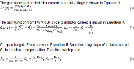
Still using the PCM CCM buck as the example, the entire regulator has been modeled into the Laplace transfer function block diagram as shown in Figure 3. There are two control loops: the voltage loop and the current loop. In the current loop, inductor current is sensed by RT and sampled into a ramp on the first negative input of the comparator. In the voltage loop, output voltage ripple is sensed by the resistor divider with a gain of K and sampled into the compensator network Av(s) as error voltage into the comparator’s positive input. With the slope compensation ramp as the second negative input signal, the comparator generates a regulated duty cycle signal into the average small signal model of the power stage to modulate inductor current.


