 A ball grid array (BGA) is a type of surface-mount packaging used for integrated circuits. BGA packages are used to permanently mount devices such as microprocessors. A BGA can provide more interconnection pins than can be put on a dual in-line or flat package, each pin is provided with a solder ball. All connections are distributed in a uniform surface grid or matrix on the component. The whole bottom surface of the device can be used instead of just the perimeter.
The leads are also on average shorter than with a perimeter-only type, leading to better performance at high speeds.
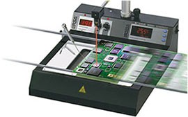
Soldering of BGA devices requires precise control and is usually done by automated processes. BGA devices are not suitable for socket mounting.
The advantage of BGA
- Efficient use of PCB space. Using BGA packages means fewer component involvement and smaller footprints, it is also help to save space for custom PCBs, which greatly increases the effectiveness of PCB space.
- Improve thermal and electrical performance. Due to small size of PCB base on BGA package, heat dissipation is more easily. When silicon wafer is mounted on top, most heat can be transmitted down to the ball grid. When silicon wafer is mounted on the bottom, the backside of the silicon wafer connect to the top of the package and is considered to be one of the best heat dissipation methods. The BGA package has no pins that can be bent and broken, which makes it stable enough to ensure large-scale electrical performance.
- Improve manufacturing profit based on welding improvement. Most BGA package pads are large, which makes large area soldering easier and more convenient. As a result, the manufacturing speed of PCB increased with the increase of manufacturing yield. In addition, when using larger pads, it is easily to re-work.
- Less damage. BGA leads consist of solid solder balls that are not easily damaged during operation.
- Reduce costs. All advantages shown above help to reduce costs. Efficient use of PCB space provides opportunities to save material, while improving thermoelectric performance helps ensure the quality of electronic components and reduce defects.
BGA technology
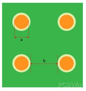
The usually BGA technology of PCBWay are minimum size 0.3mm, the minimum distance to circuit line is 0.2mm,the minimum distance between two BGA is 0.2mm. If you need higher requirement, please make a note.
 BGA Assembly Capabilities
Four automated placement systems available with Vision Systems capable of inspecting solder ball coverage. One automated
systems available with 3-D laser capable of inspecting solder ball height Automatic placement of CBGA, PBGA and MBGA
Verification of BGA’s using Phoenix real-time x-ray system. Ball Grid Array (BGA) style circuit boards, which used small circular balls
of solder to allow the flow of electricity between parts of the circuit. This brought with it a number of advantages to PCB assembly:
Higher-density circuits: As through-hole circuits were more densely-populated, soldering them accurately without crossover or short-circuits became nearly impossible. Heat conduction: BGA circuits allow heat to pass much more easily from the integrated circuit outwards, reducing overheating problems. Lower inductance: Because each solder ball in an BGA circuit is generally only a handful of millimeters large, problems from interference within the circuit are
greatly minimized.
Free PCB assembly quotation is just a click away. Click HERE to enter our PCBa Price Calculator, fill out your custom PCBa spec, and rough PCB price will show up in the right column automatically (shipping price will be given on order confirmation page).


