
Source : IC Insights
Semiconductor manufacturers closed 72 wafer fabs from 2009 to 2013 and another nine fabs are scheduled to close in 2014, according to IC Insights. The hardest hit were 150-mm wafer fabs as suppliers looked to gain greater efficiencies.
The Global Wafer Capacity 2014 report finds the semiconductor industry has closed or repurposed older capacity ≤200-mm wafer fabs to produce devices more cost-effectively on larger wafers since mid-2007. Some of the wafer fabs have been refurbished for production using larger wafers or for production of “non-IC” products. One example cited in the report is a 300-mm wafer fab operated by Sony that was initially closed then retrofitted to manufacture image sensors for the company.
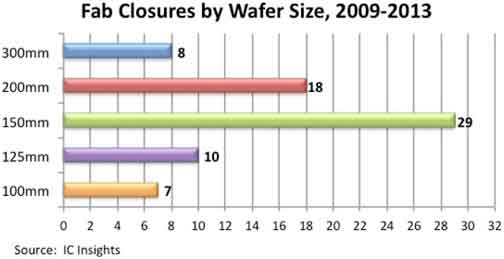
The report indicates that 40 percent of the fab closures since 2009 have been 150-mm wafer fabs. Qimonda was the first company to close a 300-mm wafer fab after it went out of business in early 2009, and both ProMOS and Powerchip closed their 300-mm wafer fabs in 2013.
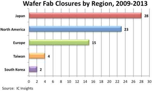
By region, semiconductor suppliers in Japan have closed 28 wafer fabs since 2009, more than any other country/region over the past five years, said IC Insights. North American suppliers shuttered 23 wafer fabs and Europe closed 15 fabs.
IC Insights reports nine fabs have closed or are expected to close in 2014. These include the following:
- Intel’s Fab 17 (200 mm) in Hudson, Mass.
- International Rectifier’s 150-mm Fab 10 in Newport, South Wales
- Renesas Electronics’ three fabs (two 150 mm, one 125 mm)
- NXP’s 100-mm and 150-mm wafer fabs in Nijmegen, The Netherlands
- Panasonic Semiconductor’s 75-mm wafer GaAs fab to produce optoelectronic devices
The two NXP fab closures were expected to be finalized in 2011, but were delayed due to strong demand for analog and logic ICs and some discrete components that are manufactured at these facilities, said IC Insights. A 200-mm fab continues to operate in Nijmegen.
Analysts expect several more companies to close older fabs and transition to a fab-lite or fabless business model in the coming years as the cost of new wafer fabs and manufacturing equipment continues to increase.


