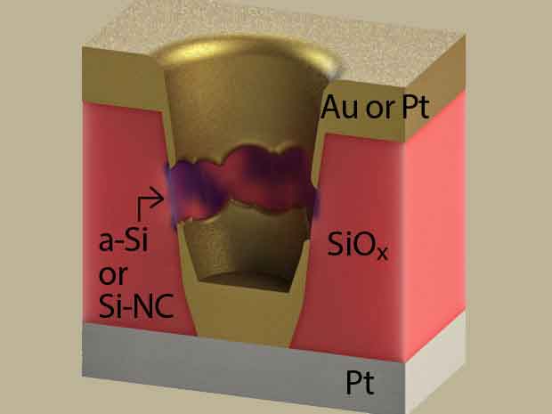
Resistive random-access memory (RRAM) has promised a new generation of computer memory by decreasing the size of memory cells through the storage of data as resistance rather than charge. With RRAM, a dielectric material is sandwiched between two electrodes so that when a voltage is applied ions are pulled from one of the electrodes, forming conductive filaments that lower the cell’s resistance.
Research has focused on finding the best material for the dielectric, and a wide variety of materials are being pursued, including paper.
Since 2010, James Tour and his colleagues at Rice University have been pursuing silicon dioxide as the dielectric material for a RRAM cell after they discovered conductive filament pathways can be formed in the material. Now Tour and his colleagues have taken another step in making silicon oxide the basis for high-density, next-generation computer memory.
The Rice team has refined the production of the memory cells to make it possible to fabricate the devices at room temperature with conventional production methods.
Companies are looking to win at RRAM using a variety of materials, such as Panasonic’s use of tantalum oxide and others the development of hafnium oxide. But Tour and his colleagues recently published a paper in the journal Nano Letters that makes the case that nanoporous silicon oxide is superior to the other technologies.
“Our technology is the only one that satisfies every market requirement, both from a production and a performance standpoint, for nonvolatile memory,” Tour said in a press release. “It can be manufactured at room temperature, has an extremely low forming voltage, high on-off ratio, low power consumption, nine-bit capacity per cell, exceptional switching speeds and excellent cycling endurance.”
Tour comes to this conclusion after the latest version of silicon oxide produced by the Rice researchers exceeded previous versions in a number of important performance parameters. The Rice team used a nanoporous version of silicon dioxide that reduced the amount of voltage needed to create the conductive pathways down to less than two volts. This represents a 13-fold improvement over the team’s previous best. And it brings silicon oxide right back into the running against competing materials.
The researchers were also able to eliminate the need to fabricate so-called device edge structures. “That means we can take a sheet of porous silicon oxide and just drop down electrodes without having to fabricate edges,” Tour said. “When we made our initial announcement about silicon oxide in 2010, one of the first questions I got from industry was whether we could do this without fabricating edges. At the time we could not, but the change to porous silicon oxide finally allows us to do that.”
The advantages of switching to a nanoporous variety of silicon oxide didn’t end there. The new porous version allows the cell to endure 100 times as many write-erase cycles as the previous version. Additionally, the porous silicon oxide cell’s capacity to hold up to nine bits is the highest number among oxide-based memories, the Rice team claims.
The research team reports that they have already received overtures from companies interested in licensing the technology.


