According to Prismark Partners, the use of quad-flat no-leads (QFNs) is growing faster than any package type except for flip-chip CSPs. Prismark projects that by 2013, 32.6 billion QFNs will be assembled worldwide, which represents 15% of all IC packages.
However, QFNs can be a challenge to assemble, especially when it comes to voiding. In most QFN assembly processes, solder paste is used as a means of attachment. This approach can be problematic, as excessive voiding often occurs due to the lack of standoff on the component and the high flux content of the paste. The addition of a solder preform can reduce such voiding by increasing the solder volume of the joint without adding flux volume.
Adding preforms to an assembly process is very easy. Preforms are packaged in tape & reel for easy placement by standard pick and place machines, right next to your components. The focus of this paper will quantify the preform requirements and process adjustments needed to use preforms in a standard SMT process. In addition, experimental data showing void reduction using preforms will also be presented.
Authors:
Seth Homer, Assistant Product Manager for Indium Corporation
Ronald C. Lasky, PhD, PE, Senior Technologist, Indium Corporation


Advances in flux formulations and particle size distribution have led to increased capabilities for solder paste; however, there are some challenges that still exist, especially as related to specific components. One component in particular is quad-flat no-leads (QFNs).
QFNs are close to the size of a chipscale package. In addition to having no leads, QFNs have a thermal pad to conduct heat out of the integrated circuit (IC) in the QFN into the printed wire board (PWB). Figure 1 shows a QFN with its leads and thermal pad.

QFN packages are slated to have one of the highest growth rates in the next few years, predicted to be over 15% per year by Prismark Partners. This growth is understandable as QFNs are desirable for assembling miniaturized personal electronic devices such as mobile phones. With approximately 6 billion worldwide mobile phone subscriptions, a number approaching one-half of the world’s population, mobile phones are rapidly becoming the defining electronic device of this era. So, miniaturized packages, such as QFNs, will continue to be in demand into the foreseeable future.
Unfortunately, when assembling QFNs, voids can form in the reflowed solder paste under the thermal pad. This paper will review steps to minimize this type of void formation by using solder preforms.
How Voids Form in QFNs
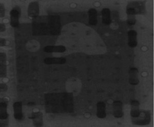
In the typical QFN assembly process, solder paste is printed on the PWB lead pads, as well as the PWB pad for the QFN thermal pad. The QFN component is then placed. The QFN design leaves little vertical space between the QFN thermal pad and the PWB pad. Therefore, during the reflow process, it is difficult for all of the flux volatiles to escape from the area of the QFN thermal pad. This phenomenon is exacerbated by the fact that solder paste is approximately 50% flux by volume. As a result of these trapped volatiles, voiding is common (see Figure 2).
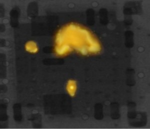
In addition to this concern, some QFN designs are too large and demand more solder than printed paste can deliver to the solder joint. In these cases, the lack of solder is responsible for the voiding, which can result in poor thermal conductivity between the QFN pad and the PWB. This poor thermal conductivity can lead to the IC overheating and can then cause near term IC failures, in addition to long term IC reliability risk. Figure 3 shows a thermal image of such an overheating IC.
Acceptable voiding level criteria vary depending on the component and the application, but the most common QFN concern is with the largest void created on the thermal pad. A solder preform, in conjunction with the paste deposit, will assist in reducing the size of these large voids, as well as reducing overall quantity of voids.
A QFN Voiding Solution Using Solder Preforms
Approaching a solution using a solder preform requires attention to the following areas:
- Stencil design
- Preform geometry
- Placement parameters
- Preform flux coating
- Reflow profile
Stencil Design
Stencil design parameters vary when using a solder preform. However, results indicate that stencil designs that maximize the solder paste under the component result in less voiding, indicating that a maximum amount of solder is required under the QFN. Following the QFN manufacturer’s design recommendations is a good starting point.
Preform Geometry
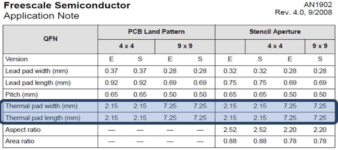
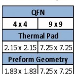
Experimentation has shown that the best results are achieved when the solder preform occupies approximately 80 to 85% of the area of the PWB pad, and is approximately 50% of the printed paste thickness. However, a minimum preform thickness of .0015” is required to prevent preform bending.
Table 2 shows typical preform and pad metrics.The ratios in this table are not fixed; they are merely a starting point. For instance, a larger pad area might require a solder perform closer to 80% of the pad area. However, the solder paste must provide tack for the preform and the QFN.
Therefore, allowing for paste around the perimeter enables the solder paste on the edge of the preform to provide good tack to the QFN. This will help prevent skewing during reflow.
Placement Recommendations

Since the solder preform is packaged in tape & reel, its placement can be manipulated easily to achieve the desired result. In order to ensure there will be sufficient tack to hold the QFN component, the preform must be pushed into the paste far enough to allow for the solder paste contact to the QFN (see Figure 4). If this result isn’t achieved, component floating will occur. The solder preform placement force is critical, as the preform still needs to be as flat as possible after it is placed into the paste. In addition, component placement pressure should be increased to ensure that the component seats well in the paste along the perimeter of the preform (see Table 3).

Increased placement pressure on the solder preform can result in its bending. The pick & place nozzle should occupy the most surface area possible on the preform (see Figure 5). The best nozzle will support the preform to preserve flatness, as bending can result in skewing of the QFN at reflow.

Flux Coating
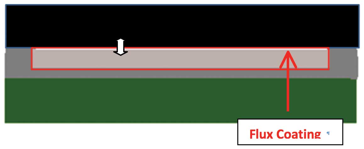
The interface between the top of the solder preform and the thermal pad on the QFN does not contain paste; therefore, there is no flux to prepare the surface for solder wetting. This shortcoming can also cause excessive voiding. The solution is a flux-coated solder preform (see Figure 6). A solder preform, coated with NC-9 flux at 1 to 1.5% by weight, will be sufficient to ensure good wetting without incurring voiding. The flux coating must be deemed compatible with the paste used.
Reflow Profile
When adding a solder preform to the process, reflow profile adjustments are not specified or required. In cases of low thermal mass, a more linear profile is acceptable, but in cases of high thermal mass, a soak profile is required. The addition of a solder preform has actually been shown to reduce variability from one board to the next and is tolerant of reflow profile adjustments.
Collaborative Testing Overview
In order to evaluate the effectiveness of solder preforms in minimizing voiding in QFNs, a collaborative investigation was performed. The critical parameters in this study are listed below:
- QFN thermal pad dimensions (dims): 2mm x 2mm
- Paste: No-clean solder paste with 89% SAC387, Type 3
- PWB pad dims: 2mm x 2mm
- Stencil dims: 2mm x 2mm x .004” thick
- Preform dims: 1.7mm x 1.7mm x .002” thick
- Flux coating: NC-9 @ 1.0% by weight
- Profile: Soak
The resulting voiding average was less than 10% and improvement from the initial voiding average can be as much as 50% or more of the solder joint.
Conclusion
As stated, voiding under QFNs is attributed to flux entrapment and/or lack of solder in the joint. The addition of a solder preform dramatically increases the solder content without excessive flux. The additional solder density residing in the center of the pad also inhibits the development of a large void.
To minimize voiding, design considerations should include:
- Stencil design: manufacturer recommended
- Solder preform geometry: approx. 85% thermal pad dimensions and 50% paste thickness
- Placement parameters: increase placement pressure, muzzle selection
- Flux coating: required for solder preform/QFN interface
- Reflow profile: dependent/flexible
This paper was first published at SMTAi, October 2011.


