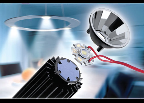
Microelectromechanical Systems (MEMS) are micron-size devices that can sense or manipulate the physical world. MEMS are recognizing potential scope in LED and LED packaging applications as LED lighting system costs can be reduced with good control circuit design and component selection. This exclusive study will bring out latest innovations and trends in MEMS when considered for LED businesses.
 Recent innovations in LED technologies have seen a new type technology of a wafer level packaging method for LED with aspheric lens and microlens array using microelectromechanical systems (MEMS) technology and transfer molding process.
The novel packaging structure includes two components: the silicon-based packaging substrate which is formed with arrayed reflector depression and through-hole interconnects by bulk micromachining and the optical encapsulation with lens configuration that formed by transfer molding in wafer level. By this pattern transfer process, the precise alignment between lens configuration and the reflector of silicon substrate can be achieved and batch process can be realized to reduce the costs. Beside, the packaging element can be used more applications. In the study, the pattern transfer of various lens profiles was also accomplished successfully by using silicone gel as lens mold. The brightness of the packaging elements with single aspheric lens profile and high fill factor microlens array can be increased by 26% and 16%, respectively, in comparison to the case of optical encapsulation with smooth curved surface.
Furthermore, the light radiation uniformity was improved effectively through 100% fill factor microlens array. Therefore, the structure can satisfy the requirements of wafer level LED packaging and
improve the heat dissipation and light extraction efficiency.
MEMS business overview
In 2014, the MEMS sector represented an $11.1B business for Si-based devices as per Bosch Ltd. The
MEMS industry has reached this landmark thanks to the smartphone and tablet industry and there’s still
growth ahead for wearables and the ‘Internet of Things’ (IoT). Meanwhile, the industry is proving to
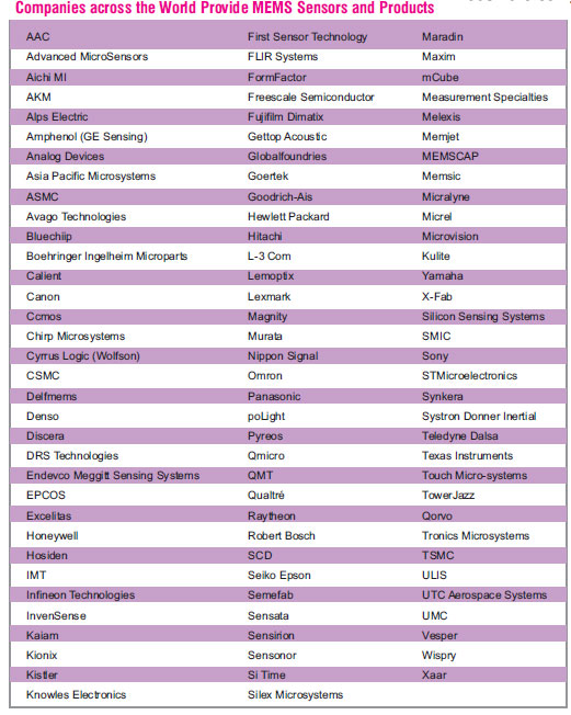
be highly dynamic. Even the more mature markets such as automotive are calling for new technologies to meet their challenges. With a production cost of only a few tens of cents for some devices, motion sensing is becoming a commodity as cheap as temperature sensors were a few years ago. And mature processes are opening the way to larger market volumes and integration of multiple sensors in a system or even in a single package. It also may soon be time for a shift to larger wafer sizes. Furthermore, MEMS is an exploring new area that call for reduced size by half or more and also cutting costs, thus opening up new opportunities like LEDs. MEMS have always relied on using semiconductor micro-machine based technologies to create devices that replace more complex and bulky or less sensitive devices. Anticipated by experts, 300mm MEMS manufacturing will be an interesting topic in coming years. The move to
300mm production could impact the entire MEMS supply chain from R&D through design, material and chemicals, equipment, and packaging. We believe one main motivation will be technical requirements, such as having a CMOS layer with a small critical dimension as required by the increasing amount of data to process. Another motivation will be economic, as companies aspire to lower costs, increase volumes and for foundries attract more customers. Packaging has been the focus of many MEMS players, but now software is also becoming a crucial part of the final MEMS sensors. With further integration of sensors, ever more data needs to be processed and software allows multi-axis detection when packaging cannot
shrink the sensor enough, as in mCube’s sensors. As software is an essential part of future sensors,
this is fuelling acquisitions, like Invensense’s move for Movea. These advances, along with the development of NEMS, new packaging and other factors will drive new investment cycles for MEMS.
MEMS and LED applications
LED lighting system steered by low power, innovative usage and small foot-print is on a drive to popularity and participating in major share of lighting business. More and more commercial contractors are installing low-power lighting in the drive to reduce energy costs and shrink carbon footprints, but automation and intelligent control offer further savings by switching off services in unused areas. Lighting accounts for about 25% of the commercial building sector’s energy use and, although it is less significant in the home, this remains one of the easiest ways for end-users to reduce their costs. Switching to less power-hungry light sources, such as compact fluorescent lighting and LEDs, is having a huge impact on energy use and cost, but domestic and business users can reduce costs further by improving control and
applying automation. This call for automation will ask lots of sensors to work in parallel and MEMS sensors is answer to the LED based networks. Lighting controls offer significant potential for
reducing that energy use, and technologies like MEMS sensor are making a wide range of innovative strategies possible, from room-level awareness of occupancy and daylight sensing, to building-wide coordination of a fully networked system. From household to industrial lighting perhaps the greatest potential for energy savings comes from the ability to automatically switch lights off when they are unnecessary and on when they are required. This is the drive behind a resurgence of interest in infrared MEMS sensors. MEMS sensor technologies, capable of detecting stationary heat-emitting objects, are able to take a larger share of the opportunities this growth brings by occupying territory inaccessible to the familiar PIR detector, traditionally used for presence detection in home and building automation systems. MEMS thermopiles, essentially nano-scale arrays of thermocouples, measure the actual temperature of the sources rather than a differential value, so they detect people in a room even when they are not moving. Presence detection opens whole new applications that motion-detecting
pyroelectric sensors cannot touch. For example presence detectors can be used as inputs to lighting, reliably switching to energy saving modes when there are no people in the zone that is being monitored. Indeed the applications extend out to heating, air-conditioning and security systems. MEMS sensors, like Omron’s D6T, measure temperature across the whole field of view. Compare that with conventional thermal sensors, which are restricted to measurements at a single point. Configured as an array (1×8 and 4×4 arrays are available currently), the sensor can assign temperature information to a specific cell, adding a positional dimension to its presence and temperature data. The result is higher accuracy, lower crosstalk and a wider field of view. Using several sensors in a room multiplies these benefits: a quad 4×4 array sensor modules can be used to obtain higher resolution or broader coverage, for example, identifying a person’s location within 1m across a 16m² area. The technology behind these new thermal sensors combines a MEMS micromirror structure for efficient IR radiation detection with a high-performance silicon lens to focus the infrared rays onto its thermopiles. Proprietary application-specific integrated circuits then make the necessary computations and convert sensor signals into meaningful digital outputs. The result is +/- 0.14 C° resolution with noise immunity (measured as noise equivalent temperature difference) of 140mK. Larger 16×16 MEMS sensor arrays are currently being developed, which will provide finer lighting control, especially in open space environments.
Today, the MEMS & sensors industry faces new challenges like cost & size reduction, reduced timeto- market, maintaining sensor value, and offering new functionalities. These challenges are mostly driven by consumer and portable/wearable electronics applications. Solutions to overcoming these challenges include:
- Developing excellence in high-volume manufacturing
- Offering more software for increased addedvalue
- Developing new detection principles
It is challenging to continue reducing size at the sensing element level, since inertial will always require a minimum mass to detect movement. Also, there is a limit to how low cost can go. Today, we see two ways to further push MEMS miniaturization and cost reduction. One way is to bolster MEMS process optimization with 3D integration and new wafer bonding approaches. Since 2010, MEMS innovation has occurred at the packaging level. For example, Through Silicon Vias (TSV) technology was introduced by STMicroelectronics in 2012 for accelerometers. Today, both mCube and Robert Bosch are using TSV to achieve very small devices.
Through 3D integration, significant size reduction has been achieved with a smaller sensing area, and, in the future, a slight reduction of MEMS structure could be achieved in subsequent generations (i.e. with more precise etching technologies, thicker proof masses, etc.). However, the wellknown MEMS law of “One MEMS, One Process” still rules MEMS production. This strongly impacts manufacturing since any introduction of new materials means a new process must be developed. This task is more easily achieved by a newcomer rather than an established player with proven manufacturing platforms and well-established yields. Thus, innovation could come from small,
Forward thinking MEMS companies and R&D labs that are developing tomorrow’s sensing technologies. Employing detection principles is the second breakthrough approach for continued MEMS & Sensors innovation.


