-
Latest Version Supports New Lattice CrossLink-NX FPGAs
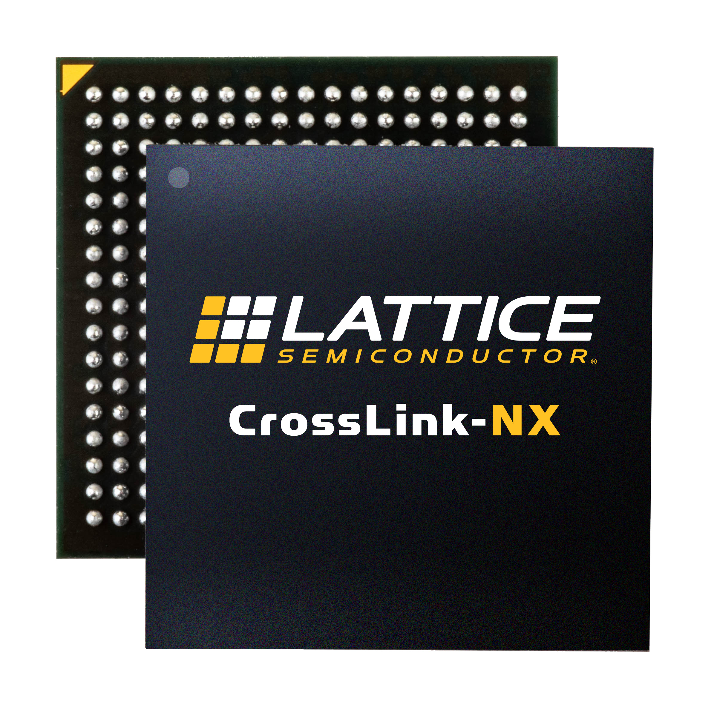
 HILLSBORO, OR – December 10, 2019 – Lattice Semiconductor Corporation (NASDAQ: LSCC), the low power programmable leader, today announced the availability of the latest version of its popular software design tool for FPGAs, Lattice Radiant™ 2.0. In addition to adding support for higher density devices like the new CrossLink-NX™ FPGA family, the updated design tool also offers new features that make it faster and easier than ever to develop Lattice FPGA-based designs.
When system developers evaluate hardware platforms, the actual hardware is only a part of their selection criteria. They also evaluate the design software used to configure the hardware for its ease-of-use and supported features, as these features can have a significant impact on overall system development time and cost.
Roger Do, Senior Product Line Manager, Software at Lattice said, “Lattice Radiant 2.0 design software gives developers an easy-to-follow user experience; the tool leads them through the design flow from design creation, to importing IP, to implementation, to bitstream generation, to downloading the bitstream onto an FPGA. Developers with little to no experience working with FPGAs should be able to quickly leverage the automated features of Lattice Radiant. For experienced FPGA developers, Lattice Radiant 2.0 allows for more granular control over FPGA settings if specific optimizations are required.”
New feature upgrades available in Radiant 2.0 include:
- An on-chip debugging tool that allows users to conduct bug fixes in real time. The debugging feature lets developer insert virtual switches or LEDs in their code to confirm viability. The tool also lets users change hard IP block settings to test different operating modes.
- Improved timing analysis provides more accurate trace and route planning and clock timing to avoid design congestion and thermal issues.
- The engineering change order (ECO) editor lets developers make incremental changes to a completed design without having to recompile the entire FPGA database.
- The Simultaneous Switching Output (SSO) calculator analyzes the signal integrity of individual pins to ensure their performance isn’t adversely affected by their proximity to another pin.
For more information, please visit www.latticesemi.com/LatticeRadiant.


