Virtex-7 Boards Offered in XMC and VPX Form Factors
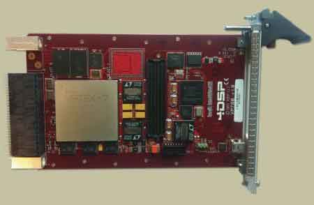
Two highly configurable modules feature advanced digital signal processing (DSP) capabilities and multiple I/O options and are available from 4DSP in both 3U VPX and XMC from factors. The FM780 is XMC (VITA 42.3) compliant with a PCI Express Gen 2 interconnect while the VP780 is 3U VPX form factor (VITA 46) compliant. Both modules provide an FMC (FPGA Mezzanine Card, VITA 57) site and two 4DSP Board Level Application Scalable Technology (BLAST) locations that are closely coupled to the onboard Xilinx Virtex-7 FPGA, and 2 Gbytes of DDR3 SDRAM.
The Virtex-7 FPGA device available on board is user-programmable and can implement high-end signal processing algorithms. Based on customer requirements, front-panel I/O modules may be added to enable the FM780 or VP780 to perform data acquisition and waveform generation, high-speed communication, image processing, and implement various types of complex DSP applications. In addition to 2 Gbytes of onboard DDR3 SDRAM, the FM780 and VP780 have a variety of memory options such as NAND Flash, QDRII SRAM+ and extra DDR3 SDRAM through BLAST modules. Optionally, the user-configurable BLAST mounting sites may be populated with JPEG2000 CODECs or even a customer’s specific logic devices or circuit designs. Both the FM780 and VP780 are available as conduction-cooled modules. (Figure 1)
4DSP
www.4dsp.com
XMC Links Virtex-6 FPGA to PCIe, SRIO and Gbit Ethernet
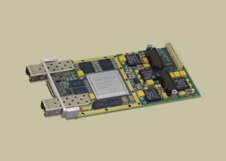
Acromag’s XMC-6VLX mezzanine modules feature a configurable Xilinx Virtex-6 FPGA enhanced with multiple high-speed memory buffers, I/O and numerous high-bandwidth serial interfaces. The FPGA provides rapid processing and is closely coupled to the serial interconnects to prevent data transfer bottlenecks. 10Gbit Ethernet, PCI Express, Serial RapidIO and Xilinx Aurora implementations are supported. Optional front-panel I/O adds dual SFP ports for Fibre Channel or copper Gbit Ethernet and a VHDCR connector for expanded I/O signal access. Typical uses include simulation, communications, signal intelligence and image processing.
Build options include the choice of a Xilinx XC6LX240T or XC6LX365T FPGA device and additional front-panel I/O connectors. Base models are ready for use in air-cooled or conduction-cooled systems. The front I/O option adds two 2.5 Gbit/s SFP connectors and a 36-pin VHDCR connector for JTAG, USB and 22 SelectIO. SelectIO signals are Virtex-6 FPGA I/O pins that support single-ended I/O (LVCMOS, HSTL, SSTL) and differential I/O standards (LVDS, HT, LVPECL, BLVDS, HSTL, SSTL). All models are available with extended temperature range parts suitable for -40° to 85°C operation.
The rear I/O supports 8-lane high-speed serial interfaces on both the P15 and P16 XMC ports for PCI Express, Serial RapidIO, 10 Gigabit Ethernet, or Xilinx Aurora implementation. P16 also has 34 SelectIO channels and two global clock pairs direct to the FPGA. The P4 port adds another 60 SelectIO and two more global clock pairs. Available in a variety of configurations, models start at $8,250 with upgradeable logic, I/O and operating temperature capabilities. (Figure 2)
Acromag
www.acromag.com
6U OpenVPX Card Has Stratix V FPGAs and Anemone Coprocessors
BittWare offers a 6U VPX board powered by Altera’s 28-nm Stratix V FPGAs. The S5-6U-VPX (S56X) is a rugged VITA 65 6U VPX card providing a configurable 48-port multi-gigabit transceiver interface supporting a variety of protocols, including Serial RapidIO, PCI Express and 10GigE, and two VITA 57 FMC sites for enhancing the board’s I/O and processing capabilities. When combined with the optional BittWare Anemone floating point coprocessors, the board packs a powerful punch for those applications requiring flexible FPGA processing in a rugged form factor.
By leveraging the Stratix V GS FPGA’s floating point DSP blocks, which deliver up to one TeraFLOP of computing performance, combined with the FPGA’s low-power, multi-gigabit transceivers and a high-density, high-performance architecture, BittWare’s S56X board delivers a rugged and completely flexible signal processing solution capable of driving innovative new capabilities in military applications. The board also sports an 800 MHz ARM Cortex-A8 control processor and two Anemone floating point coprocessors (optional). I/O includes 48 multi-gigabit transceivers along with GigE, SerDes, LVDS and RS-232 links. Up to 8 Gbytes of onboard DDR3 memory are also included. (figure 3)
BittWare
www.bittware.com
ADC/DAC 6U VPX Module Targets Electronic Warfare Applications
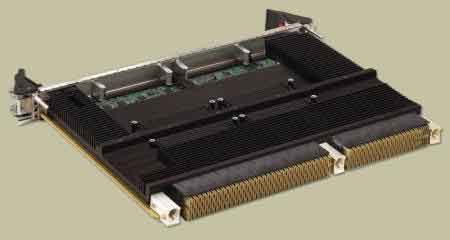
Applications like electronic warfare have a huge appetite for low-latency, high-ADC/DAC performance combined with the highest available I/O bandwidth. With that in mind, Curtiss-Wright Controls has introduced the CHAMP-WB (“WideBand”), the Industry’s first Xilinx Virtex\-7 OpenVPX COTS DSP Engine designed for sense-and-response applications that require high bandwidth and minimal latency. In addition, Curtiss-Wright is also introducing its first module for the CHAMP-WB, the TADF-4300, featuring Tektronix Component Solutions’ 12.5 Gsample/s ADC and DAC technologies.
Combined, these two modules form the CHAMP-WB-DRFM and provide the highest bandwidth/highest resolution platform for wideband Digital Radio Frequency Memory (DRFM) processing available in the embedded defense and aerospace market, delivering an unprecedented 12.5 Gsamples/s 8-bit ADC and 12.5 Gsample/s 10-bit DAC performance from a single 6U slot. Based on Tektronix’s silicon germanium (SiGe)-based data converters, the TADF-4300, when coupled with the CHAMP-WB’s onboard Virtex7 FPGA and high-speed wideband interfaces, enables designers to develop powerful embedded DRFM solutions with 3x the performance of existing CMOS-based offerings. Memory support on the CHAMP-WB includes two 64-bit, 4 Gbyte DDR3L memory banks that provide up to 8 Gbytes of on-card data capture or pattern generation capability. (Figure 4)
Curtiss-Wright Controls Defense Solutions
www.cwcdefense.com
3U VPX Virtex-6 FPGA Processing VITA 57 FMC Front-End
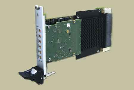
VPX and FMC are two of the fastest growing new embedded computer form factors, and the military has its eye on both. Hitting both of those trends, Elma Electronic offers the TIC-FEP-VPX3b, an FPGA-based 3U VPX front-end processing board that provides an FMC site coupled to a large capacity Virtex-6 FPGA for extremely flexible I/O. Designed for digital signal processing (DSP), the versatile TIC-FEP-VPX3b is ideal for applications such as radar, sonar, electronic warfare, imaging and communications. The new board offers high-performance logic, increased SerDes-based I/O, and powerful DSP slice resources that help meet higher bandwidth and performance demands, while utilizing up to 25% less power.
Supported by low-power and high-speed GTX transceivers at rates up to 6.5 Gbits/s, the board enables the application of interfaces used in today’s embedded systems. Onboard PCIe Gen 1 and Gen 2 protocols, via a hard IP block and Ethernet MAC blocks, allow PCIe x4 and GbE interfaces to be implemented from the FPGA to form data and control planes respectively. Built to the VPX specifications, the TIC-FEP-VPX3b includes four 4-lane fabric ports on the P1, connected by GTX transceivers to the main FPGA. Featuring an onboard Xilinx Virtex-6 FPGA, the board comes with two banks of 40-bit 1.25 Gbyte DDR3 memory with transfer rates of 7.5 Gbits/s and a Spartan-6 control node used to load logic images into the main FPGA. The Spartan-6 control node enables “on the fly” bitstream management for dynamic FPGA configuration. Other resources include zero bus turnaround (ZBT) SRAM with a throughput of 400 Mbyte/s for expedited read/write processing. The board comes in three environmental grades: standard, rugged and conduction-cooled. Pricing for the TIC-FEP-VPX3b depends on the choice of Xilinx FPGAs and environmental grade. The board is currently shipping. (Figure 5)
Elma Electronic Systems
www.elma.com
Xilinx Virtex-7 FPGA-Based XMC and VPX Modules
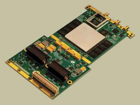
Two high-performance FPGA processing modules are now available in industry-standard XMC and 3U VPX form factors. The COTS XPedite2470 3U VPX and XPedite2400 XMC modules from Extreme Engineering Solutions utilize the Xilinx Virtex-7 Family of FPGAs to merge high throughput, configurable I/O and DSP-level processing with high thermal efficiency. These modules can use the VITA 49 VITA Radio Transport (VRT) protocol, which provides an industry-standard framework for formatting the data of a digitized IF stream. This enables interoperability and simplifies system integration because, prior to the release of VRT, each receiver manufacturer would implement its own proprietary digitized formats. Additionally, VRT data can be carried over commonly used industry-standard protocols, such as Gigabit Ethernet, 10 Gigabit Ethernet, PCI Express, Aurora, Serial RapidIO (SRIO) and Serial Front Panel Data Port (S-FPDP).
The XPedite2470 is a configurable, 3U VPX-REDI, FPGA-processing module that provides eleven high-speed GTX lanes to the backplane and eight high-speed GTX lanes to an on-card FMC site. It includes a Freescale P1010 QorIQ processor for additional signal-processing or general-purpose capabilities. The compact XPedite2400 is an FPGA-based XMC module that includes a high-speed DAC, 2 Gbyte of DDR3 SDRAM, a Gen3 PCI Express interface and up to ten high-throughput GTX lanes. The module’s integrated DAC supports a 14-bit resolution and a sample rate of up to 2.5 Gsamples/s. (Figure 6)
Extreme Engineering Solutions
www.xes-inc.com
FPGA PMC/XMC Module Blends Digitizing and Processing
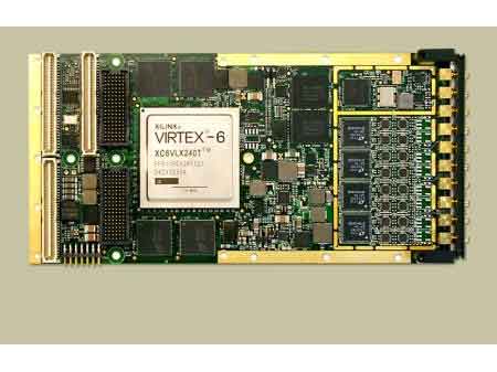
Innovative Integration has announced its X6-250M, a PMC/XMC I/O module that integrates digitizing with signal processing. The module has a powerful Xilinx Virtex-6 FPGA signal processing core and high-performance PCI Express/PCI host interface. Applications include software-defined radio, radar receivers and multi-channel data recorders. The card has eight simultaneously sampling A/D channels that sample at rates up to 310 Msamples/s (14-bit). The A/Ds have matched input delays and response. The A/D are supported by a programmable sample clock PLL and triggering that support multi-card synchronization for large scale systems.
A Xilinx Virtex-6 SX315T (LX240T and SX475T options) with four banks of 1 Gbyte DRAM provides a very high-performance DSP core with over 2000 MACs (SX315T). The close integration of the analog I/O, memory and host interface with the FPGA enables real-time signal processing at extremely high rates.
The X6-250M has both XMC and PCI interfaces, supporting PCI Express or older PCI systems. The PCI Express interface provides up to 3.2 Gbyte/s sustained transfers rates through an x8 PCIe Gen2 interface. System expansion is supported using secondary PCI Express or Aurora port used as a private data channel or second system bus. The X6-250M power consumption is 23W for typical operation. The module may be conduction-cooled using VITA20 standard and a heat spreading plate. Ruggedization levels for wide-temperature operation are from -40° to +85°C (conformal coating) and 0.1 g2/Hz vibration. (Figure 7)
Innovative Integration
www.innovative-dsp.com
XMC Module Does Advanced Mixed-Signal Processing
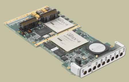
The Echotek Series DCM-V6-XMC Module from Mercury Systems implements a flexible FPGA-based architecture in a space-efficient mezzanine form factor. The modules combine the latest wideband high-performance ADC with a high-speed, high-resolution DAC, both working in conjunction with powerful Xilinx Virtex-6 technology. With this unique set of features, the Wideband DCM-V6-XMC Module delivers an ultra-high-speed digitizer and processing solution that addresses a range of demanding signal requirements.
Dual Xilinx Virtex-6 FPGAs assist with the signal processing and data movement functions, while the EchoCore FPGA Development Kit (FDK) streamlines the development of FPGA-based applications. The card does direct digitization of L-Band signals. Its advanced mixed-signal capability is suited for EW, SIGINT, ELINT, SDR, radar and wireless test and measurement. The board’s single channel 12-bit ADC samples at up to 3.6 GSPS. Another option is a dual channel 12-bit DAC at up to 1.6 GSPS. The single channel 14-bit DAC offers up to 2.5 GHz. The Virtex-6 LX240T has 241,152 logic cells, 37,680 slices and 768 DSP blocks in an 1156 pin-package FPGA. (Figure 8)
Mercury Systems
www.mrcy.com
FPGA Accelerator Card Serves Up Interfacing with Network and Storage I/O
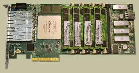
FPGA acceleration has moved beyond the benchmarking phase and is increasingly gaining acceptance for large-scale computing systems. Nallatech has announced availability of the 395 FPGA accelerator card for data-intensive network and coprocessing applications. The 395 FPGA accelerator card provides a powerful I/O and compute platform suitable for a range of applications including signals intelligence, network security and algorithm acceleration.
The four SFP+ network interfaces of the 395 enable applications that require real-time data processing, filtering and inspection of network traffic. The 395 also supports the Altera Software Development Kit (SDK) for OpenCL, which allows users to combine the OpenCL programming model with Altera’s massively parallel FPGA architecture for high-performance, energy-efficient computing. This combination enables dramatic acceleration of compute-intensive applications while reducing power consumption and total cost of ownership. An 8-lane PCI Express 3.0 interface provides high-bandwidth communications to the host platform. Four SFP+ ports support 1GbE, 10GbE, 10G SONET and various OTU standards. Four banks of DDR3 SDRAM provide up to 16 Gbytes directly coupled to the Stratix V FPGA. Two banks of QDR-II SRAM offer random memory access. (Figure 9)
Nallatech
www.nallatech.com
Wideband Software Radio Module for UAV, Radar and Communications
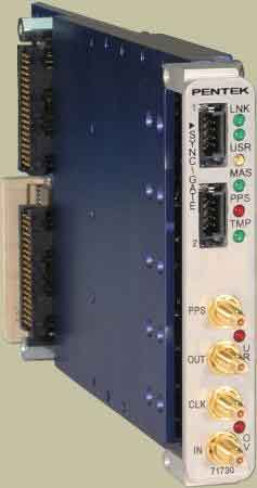
A single-channel, high-speed data converter XMC FPGA module can receive and transmit at the same sampling rate, supporting signal bandwidths up to 400 MHz. The Model 71730 from Pentek is a 1 GHz 12-bit A/D, 1 GHz 16-bit D/A module that is based on the high-density Xilinx Virtex-7 FPGA. The Model 71730 appeals to customers that need the wider symmetrical bandwidth for both input and output signals. In combination with the Virtex-7 FPGA, additional memory and the PCIe Gen 3 interface, this Onyx board offers the performance that many wideband communications systems require.
The Model 71730 comes preconfigured with a suite of built-in functions for data capture, synchronization, time tagging and formatting, making the board an ideal turn-key interface for radar, communications or general data acquisition applications. The Model 71730 features an A/D acquisition intellectual property (IP) module for easy capture and data moving and a sophisticated D/A waveform playback IP module that allows users to easily play back waveforms from onboard memory or the PCI Express interface. These modules greatly enhance the functionality of the Model 71730 and reduce the development time and effort to module deployment. Software support packages are available for Linux and Windows operating systems. Pricing starts at $19,495. (Figure A)
Pentek
www.pentek.com
PCIe/104 Card Sports Spartan-6 User Programmable FPGA
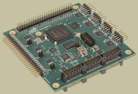
The FPGA35S6101 is a PC/104 FPGA module with a PCIe/104 stackable bus structure. This module provides a platform for customer developed FPGA code. It is based on a Xilinx Spartan-6 with a hardware PCIe x1 endpoint to provide an interface to the host CPU. On-board DDR2 memory provides dedicated storage space for the FPGA application. This board features four RS-232/422/485 transceivers connected to FPGA pins which enable custom serial port implementations.
A total of 96 I/O pins interface the FPGA to the outside world, and allow for a variety of signal levels including 5V tolerant LVTTL, LVDS, and RS-232/422/485. The Spartan-6 device offers 101,261 logic cells and 5,800 Kb of internal RAM. Example FPGA code is included to demonstrate I/O pins, DDR memory, and the PCI Express interface. With a -40 to +85°C operating temperature, this embedded FPGA board is ready for deployment in a variety of military and industrial applications. (Figure B)
RTD Embedded Technologies
www.rtd.com
VXS/VME Board Provides High-Speed 12-Bit ADCs and DACs
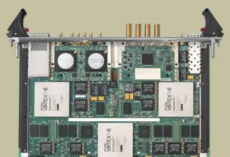
VXS continues to provide a “here and now” solution for high-speed VME-based military embedded computing. Feeding that need, TEK Microsystems has announced the latest member of our QuiXilica product family. The new Gemini-V6 supports either one 12-bit analog-to-digital converter (ADC) input channel at 3.6 Gsamples/s (GSPS) or three input channels at 1.8 GSPS, combined with a 12-bit DAC output channel operating at up to 4.0 GSPS.
Gemini-V6 is based on the National Semiconductor ADC12D1800RF device, which supports either a pair of channels in non-interleaved mode or a single channel using 2:1 interleaved sampling. Gemini-V6 contains two ADC devices, supporting a total of either three channels plus trigger at 1.8 GSPS, or one channel plus trigger at 3.6 GSPS, plus a separate 12-bit DAC output channel based on the Euvis M653D that operates at up to 4.0 GSPS. The Gemini-V6 contains two front-end FPGA devices, one attached to the ADCs and one to the DAC. The front-end FPGAs can be configured with LX240, SX315, or SX475 devices, providing both the highest FPGA processing density available in any 6U form factor today as well as the only VME / VXS platform supporting Virtex-6 FPGAs.
The two front-end FPGAs are supplemented with a “back-end” FPGA that can be used for additional processing or for backplane or front panel communications. The Gemini-V6 includes six banks of DDR3 memory with total capacity of 5 Gbytes and aggregate throughput of 32 Gbytes/s, supporting a wide range of signal processing algorithms with deep memory buffering of the entire signal acquisition stream. (Figure C)
TEK Microsystems
www.tekmicro.com


