 Keith Odom, R&D Fellow, National Instruments
Much has been published recently on the death of Moore’s law. Though the more than 50-year-old observation is facing health challenges again, don’t start digging the grave for the semiconductor and electronics market. Gordon Moore, cofounder of Intel, famously observed the rate at which transistors on a semiconductor doubled, initially every 12 months and then approximately every 24 months. Despite a few minor revisions, semiconductor processing has tracked remarkably closely to that observation for decades. This “free” scaling allowed similar architectural designs to be reimplemented, which provided the lower costs, lower power, and higher speeds expected from the growing curve. Does the disappearance of this free scaling signal the end of advancements in computing? Though this threat is serious enough to inspire DARPA to increase funding for researching a post-Moore’s law world, scientists and engineers have a history of overcoming the scaling hurdles, and some innovative alternatives to pure semiconductor scaling paint a bright and interesting future. “The end of Moore’s law could be an inflection point,” said Dr. Peter Lee, corporate vice president of Microsoft Research, in the March 2016 Technology Quarterly by The Economist. “It’s full of challenges—but it’s also a chance to strike out in different directions, and to really shake things up.”
History of Breaking the Law
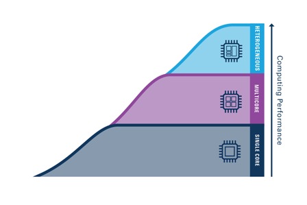
Moore’s law specifically relates to the number of transistors on a semiconductor device, but it is often confused with the other benefits of semiconductor scaling such as higher speed and lower power. These expected benefits of scaling held true for decades but are no longer easy or expected. Processor cooling stalled the exponential rise of processor frequency technology, but this apparent “wall” spurred innovations that made the multicore processor commonplace. Though core frequency growth has been limited, PC system performance has continued to scale with the addition of multiple cores and special vector processing units that speed up graphics, games, and video playback. These additions created new challenges in developing software models to best use these new processing blocks. Along with generating processing architecture changes, high-speed transistors have been applied outside the CPU to the I/O subsystems that feed the processors with higher bandwidth from networks, cameras, and data collection. Applications of high-speed signal processing to wireless and wired standards have created a growth in I/O bandwidth that has exceeded simple transistor frequency scaling.
Using the Third Dimension
Previous predictions of the end of Moore’s law have been met with breakthroughs in chip design. The current techniques to better leverage the third dimension by stacking chips and transistors will continue to increase density, but they may create new design and test problems. For example, the spiraling cost of smaller transistors has required new chips to combine more system functions to justify the higher price. This advanced “system on a chip” approach is demonstrated by the evolution of the FPGA from a simple array of logic gates into a high-performance I/O and processing system that combines processors, DSPs, memory, and data interfaces into a single chip. Many of the emerging options to scale chip density rely on using a third dimension in both how transistors are built and how 3D-IC technology can be used to combine existing chips into a single package. Though these systems on a chip are more complex to design and test, they were created to lower the end-system design cost with their high level of integration. Even with this benefit, chip stacking involves new complexities that present new challenges. As more systems rely on 3D scaling, the debug and test challenges will become more obvious, and more silicon area will be used to provide integrated debugging and test features.
New Computing Architectures
History has shown that previous scaling problems have encouraged novel architectural improvements that better leverage silicon technology. The latest challenges created the purpose-built computing era for which multiple, unique computing architecture types are combined and applied to problems. This trend grew popular with graphics processors that complement general-purpose CPUs, but that technique is rapidly expanding with custom-built computing acceleration using FPGAs, vector processors, and even application-specific computing blocks. These speed-up techniques, like those used for machine learning, will become the next standard blocks added to the system on a chip of tomorrow. The key to leveraging these mixed-processing architectures is software tools and frameworks that help users design with a high-level description for deployment to a variety of processing engines for acceleration. The initial struggle to exploit parallelism in the multicore chips will repeat as heterogeneous computing becomes the option for scaling. And though the viability of the venerable Moore’s law is being threatened again, market needs such as machine learning and autonomous driving will require continued scaling in processing capability and I/O bandwidth, which presents a fresh opportunity to drive new architectural innovations.


