By JPaul Carpenter, Mouser Electronics
I am a long-time microcontroller (MCU) person with a particular interest in using low-overhead modules to enable greater communication and interfacing than an individual chip could achieve. Some of my favorite personal projects include developing an MP3 player, an alarm clock, a wireless ground moisture control system, a dog activity monitor, and a Bluetooth low energy wireless prosthesis control. In all of these, the MCU provided both ease-of-use and the capabilities needed for gathering information and issuing simple commands.
Recently I was given a project that would not only require me to make the transition to the big, scary FPGA—Field Programmable Gate Array—but also to move into the bigger and more capable ARM cortex outside of the safety and ease of the mBed environment.,
I examined some advantages and disadvantages of FPGAs, introduced the Terasic DE10 Nano development kit, and explore example code and discover additional useful resources.
About FPGAs
If you’ve been developing projects with MCUs, you’ve probably found that the learning curve is not too steep, that tools are readily available, that development and revision processes are straight-forward, and that designs are very portable. You’ve probably also found, though, that their processing can be limited, both in terms of complexity, speed, and established interfaces. My relatively simple personal projects to date were ideal for MCUs because they were neither complex nor had significant processing needs.
FPGAs are integrated circuits that contain logic elements—with programmable building blocks already built in and are designed to be super flexible yet highly capable. For example, they can emulate microprocessors or RAM to boost performance, adapt to changes by allowing new standards or algorithms to be implemented, and add communications interfaces—all of which help reduce total system cost and extend the product lifecycle. The downside to this capability is that the learning curve is pretty steep. And for MCU developers, the learning curve is compounded by a shift in fundamental methodology in I/O and coding. Instead of a single port and voltage and instead of a single port and protocol, FPGA development allows for multiple ports with multiple voltages, can use any protocol, and processes in parallel.
Fortunately, I discovered the Terasic DE10 Nano dev kit, which is built around the Intel Cyclone® V SoC. The Intel Cyclone® V SoC combines FPGA fabric around an Dual-Core ARM Cortex A9. It makes the capabilities of the FPGA accessible by building in a number of support components, including display and communications ports, buttons/switches, pin mappings and a quick configuration tool, a JTAG debugger, and well-documented examples and guides from both Terasic and Intel.
Planning for FPGA Development
When planning for MCU development, I would determine what interfaces were needed—SPI, I2C, Wi-Fi, and so on—and then make an informed selection based on voltage, pin counts, communication interfaces, library support, and price. With an FPGA, almost every interface is now possible, but the limiting factor is the number of logic cells, which are used to create the functionality of the port, soft core MCU, or memory element. The trade-off, then, is that the higher the logic cell count, the more capable the FPGA…and the higher the FPGA cost. Although FPGAs usually have a higher initial cost they offer huge potential power and space savings as they can combine multiple components into a single component.
I found myself at a crossroads: How will I know how many logic elements I will need for my design? The answer is dictated by the needs of the FPGA intellectual property—called IP, which consist of protocols, functions, my code, and specific tasks that are normally performed by an external module. Almost all FPGAs metrics are broken down into of logic elements, registers, and total I/O banks, which are the differentiating units of measure for each chip:
- Logic Elements are the grouping of logic resources that accomplish the gate array definition of the FPGA, each with a set number of LookUp Tables (LUTs), flip-flops, and multiplexers.
- Registers are a group of flip-flops that allow data to be held between loops and enable other functions like timers.
- I/O banks are a grouping of Input-Output pins that are connected to the external world. Each bank is limited to one voltage and has current limitations.
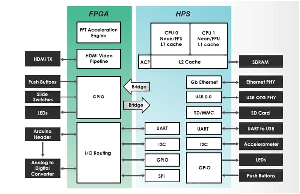
The idea of IP’s importance initially escaped me because I hadn’t yet grasped the fact that it described the ability to stand in place of a physical real-world device like an MCU, communications controller, or something I would otherwise use another piece of silicon for. Out of the box, the DE10 Nano uses the FPGA layer primarily as a very low latency I/O expansion, as shown in Figure 1. All of this, then, comes together to hit another design feature of an FPGA: It can contain most of a PCB in a single chip and thereby allow much easier flexibility in future designs.

Most of the low-level I/O is controlled and interfaced through the FPGA, giving the advantage of lowering CPU time spent waiting on a low-level I/O change. This also allows conditioning or alteration before being delivered to the hard processor system (HPS). This makes perfect sense because the Cyclone V FPGA was designed to be a fabric to expand interfacing, accelerate performance, and boost the capability of any paired HPS. In this case, as Figure 2 shows, the HDMI interface is a non-native interface to the HPS, so there aren’t many MCU resources developed for it.

At first look, I notice several positive aspects:
- HDMI output is handled on the FPGA to offload the CPU load and add a non-native interface.
- An OpenCV acceleration example exists to show the benefit of combining the two-types of processors.
- Terasic has made the basic communications available and ready to implement, and there is a predefined list of pin mappings that define the voltage and current limitations for me.
Overall, I am liking the FPGA and find the expansion and acceleration capabilities to be intriguing; however, I wonder about their limitation. How fast can they go? What protocols are supported? How many LE will they consume? Overall, the IDE is simpler than others that I have used and includes amazing documentation to get started. The hardware seems extremely robust and capable, and I am devising a project that I think will test the limits of the hardware on this board.
How do we test the hardware limits of this board?
The differences between MCU and FPGA are a bit like the differences between a scooter and a car: While both will get you from Point A to Point B, the mechanics are fundamentally different.” I thought this analogy was a good in describing the pin mode, pin types, and parallel vs. serial processing, which are quite different in FPGA as compared to MCU.
At first, I was starting with the Terasic Setup and guided practice but found that I kept getting stuck. Every time, the compiling process ended with an error. I got another cup of coffee and started going through the Intel Developer Zone website, which offered simpler examples. I was amazed at the reduction in complexity! Here, the examples were easy enough to follow that they compiled and worked. Finally, once I understood the basics, it was a lot easier to go through the Terasic examples. I think this was partly because the compilers were set up and partly because I had more familiarity with them.
The Hard Processor System
The Terasic DE10-Nano combines an MCU (the hard processor system, HPS) with an FPGA, so I decided to get started in familiar territory, the MCU. The ARM “My First HPS” development felt familiar and simple; it felt unencumbered in the Eclipse IDE; and the Intel SoC development tool helped to make programming the system a breeze. I went a little beyond the “Hello World” example and added another line to do nothing other than test the run to capabilities of the compiler…and didn’t end up with a compiler fail. The IDE was brilliant and felt very familiar to most HPS IDEs.
The FPGA
Eventually, I had to move on to the FPGA portion, where the fundamental difference is that I can do a lot of things simultaneously (or in parallel), instead of an MCU’s usually-serial fashion. Adapting to this concept felt a bit more complex and was slower, but remembering that the concept was new, it was not overly difficult. The Intel Developer Zone version is definitely the set of guides to start with, owing to the prebuilt configuration and guided installation.
The Intel Developer Zone Installation file gets the basics started, and then the Terasic builds on those new skills by bringing in additional functions and the complete process, rather than a hunt-and-peck, copy-and-paste method of learning. Intel truly introduces what I think will be the necessary knowledge base for building my own application in the near future, including building block diagrams, timing profiles, and I/O programming: The block diagrams allow a visual flow of the programming, which is useful in very complex developments. Timing profiles handle serial vs parallel and bus timing protocols that are referenced. Any pin can do anything, which is probably the most well-known feature of the FPGA. (Programming pins was a trip!) The pin allocation manager is really cool, but the table lookup is daunting. Thankfully in the newest version of Quartus, Terasic has provided a complete mapping to all the ports and pinouts using a well-documented naming schema. This makes the coding portion much easier.
Challenges Encountered
Working in a new development environment was uncomfortable. The new process and keyboard shortcuts required an adjustment, for sure and there were setup issues that usually come from setting up a new IDE. However, the documentation was clear, and the images helped a lot as well. Intel has even gone so far as to create a Linux setup and a Windows setup that gives a Linux emulation for programming, which greatly simplified the getting started process; however, I had problems with the Linux set up and gave up on my attempt at a self-compiled Linux IDE. I did, though, later find a 120-page guide to properly set it up.
The Takeaways
I enjoyed this exercise, and I feel confident in going forward. However, this phase was very heavy in downloads, configuration, and figuring out what to do next. I am stoked about the next phase where I plan on introducing different hardware, developing my own software using the example code, and taking advantage of the HPS and FPGA technology. My plan is to have the HPS run OpenCV software using external hardware and accelerate the video processing with the FPGA portion.
Stay tuned for series!
Author
JPaul Carpenter is an Electrical Engineer who works at Mouser Electronics to produce and high quality Technical Content and Projects. JPaul believes that while content may need to be technical, it doesn’t have to be unintelligible. JPaul has designed and landed custom drones as well as previously working in Human Machine Interfacing, embedded design, prosthetics research, and robotic automation research. JPaul holds a B.S. in Electrical Engineering from University of Texas at Arlington.


