
Munich, Germany – 13 March 2024 – Motor drive applications are taking a leap forward with the launch of the Infineon Technologies AG (FSE: IFX / OTCQX: IFNNY) OptiMOS™ 6 200 V MOSFET product family. The new portfolio is designed to deliver optimal performance in applications such as e-scooters, micro-EVs, and E-forklifts. The improved conduction losses and switching behavior for these new MOSFETs reduce the electromagnetic interference (EMI) and switching losses. This benefits various switching applications, including servers, telecom, energy storage systems (ESS), audio, solar and others. Additionally, the combination of a wide safe operating area (SOA) and industry-leading R DS(on) results in a perfect fit for static switching applications such as battery management systems. With the introduction of the new OptiMOS 6 200 V product family, Infineon sets a new industry benchmark with increased power density, efficiency, and system reliability for its customers’ benefit.
The OptiMOS 6 200 V portfolio delivers enhanced technical features compared to its predecessor, the OptiMOS 3. It features a 42 percent lower R DS(on) that contributes to reduced conduction losses and increased output power. Regarding diode behavior, the OptiMOS 6 200 V provides a significant increase in softness, more than three times that of the OptiMOS 3. Combined with up to 89 percent reduction in Q rr(typ), the switching and EMI behaviors are significantly improved. The technology also features improvements in parasitic capacitance linearity (C oss and C rss), which reduces oscillation during switching and lowers voltage overshoot. A tighter V GS(th) spread and lower transconductance aid in MOSFET paralleling and current sharing, leading to more uniform temperatures and reducing the number of paralleled MOSFETs.
The OptiMOS 6 200 V products feature an improved SOA and are classified as MSL 1 according to J-STD-020. These RoHS-compliant, lead-free products align with current industry standards.
Availability
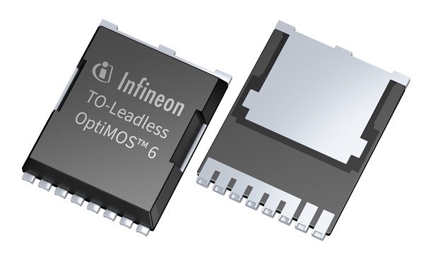
The OptiMOS 6 200 V products are available in various packages making them ideal for a broad range of applications. This wide package portfolio includes the PQFN 3.3.×3.3, SuperSO8 5×6, TOLL, TO-220, D 2PAK-7P, as well as the D 2PAK-3P. All variants can be ordered now. More information is available at www.infineon.com/optimos-6-200v.


