Jeffrey Len, Leon Rao, Evan Yin, and Wisdom Qu, Indium Corporation
As the industry is moving to smaller and finer pitches such as 008004, 0.3mm CSP, and BGA, screen printing becomes one of the critical processes to produce a good quality surface mount assembly. In this paper, we will evaluate the impact of stencil quality statistically through Minitab® software by comparing the printing performance of 0.35mm pitch and 01005 pads from different stencil suppliers.
In the era of the Internet of Things (IoT), where finer pitch components are used in applications such as mobile or system-in package devices, process control of stencil printing is important as process windows have become tighter with little to no margin for error in the process. In the past, when the process window was more “forgiving” with large aperture printing, a good area ratio of the “7 balls rule” stencil design was easily achievable and sufficient for quality printing performance. That is no longer the case, as when apertures get down to finer pitches of 01005 and 008004, other factors become critical to ensure good transfer efficiency.
Good transfer efficiency is important to provide quality printing performance. Transfer efficiency equals the percentage of actual paste volume over theoretical paste volume on a desired pad. In order to have good transfer efficiency, solder has to be deposited onto the desired area at the right volume and correct solder height. Figure 1 shows the various factors that could affect the transfer efficiency of solder paste for a typical printing application.
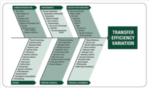 Figure 1. Cause and effect diagram for transfer efficiency.
It is widely known that solder paste selection, printing parameters, stencil aperture design (Figure 2), and printer setup are common factors that will affect printing performance, but it is still unknown as to whether the quality of stencils from different suppliers affects the solder paste transfer efficiency. Each supplier might use different laser cut equipment with varying accuracy, nanocoating material, and fabrication process. In Figure 3, the SEM images show the difference in quality produced between laser cut-polished stencils 1 and 2. In this paper, several stencil suppliers have been selected to submit two best-effort stencil types of laser cut + electropolished (EP stencil) and laser cut + electropolished + nanocoated (nanostencil). Data collected will be analyzed through Minitab® software.
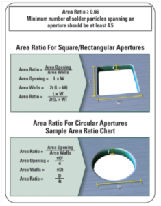 Figure 2. Area ratios for square and circular apertures
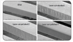 Figure 3. SEM photos of different stencil types.
Experimental Design
The focus of this experiment is to assess the impact of stencil quality on the paste’s transfer efficiency of stencils, especially on a 01005 and 0.35mm pitch BGA pad. All stencils supplied were on a best-effort basis and outgoing inspection performed per the supplier’s standard outgoing QC test. It was not within the scope of this study to verify the incoming QC test results from each supplier
Stencil Suppliers
The six stencil suppliers selected are common stencil suppliers among our customers in different regions (see Table 1). Two types of stencils were selected: lasercut electropolished (EP stencil) and laser-cut nanocoated material (nanostencil). Stencil thickness was fixed at 80 microns using SUS304 stencil material. One E-FAB stencil was used as a benchmark for this study.
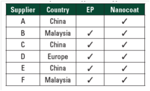 Table 1. Summary of stencil types and suppliers
Solder Paste
A no-clean, halogen-free SAC305 solder paste with a powder size particle from 15–25 microns was selected for this experiment. It is a proven solder paste within the industry with a robust printing process, and has a good transfer efficiency and response-to-pause.
Test Vehicle
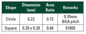
The test vehicles used in this experiment consisted of 0.35mm pitch (0.22 circles), a 01005 pad (0.20mm square), and various pads from 0.18–0.24mm in circular and square shapes. For the purpose of this study, we will focus on the data analysis of pads C0.22mm and SQ0.20mm (Figure 4).
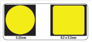 Figure 4. Stencil aperture sizes.
Stencil Design and Area Ratio
Each stencil aperture was chosen to simulate the typical pad size for 0.35mm pitch BGA and a 01005 passive component pad (see Table 2).
Printing Process
Printing parameter optimization was performed prior to the experiment, and only one printing parameter was fixed to provide a better comparison of the printing performance of each stencil. A vacuum support block and foilless clamp were used in this experiment. Understencil wipe cleaning was performed on every print and an inspection was done on the board support for every conversion to ensure proper printer setup. Below is the optimized printing parameter:
- Print speed: 50mm/s
- Print pressure: 7kg
- Print gap: 0mm
- Separation speed: 0.5mm/s
- Separation distance: 3mm
Equipment
- DEK Horizon printer
- Koh Young SPI machine
- Vacuum support
Results and Discussion
Box Plot of EP and Nanostencil on a C0.22mm Pad
Printing SPI data was collected and analyzed through a box plot to reveal the mean and STD of solder volume. Results in Figures 5 and 6 show that stencil D had the highest mean value for both the EP and nanostencil at 101.00% (EP) and 101.80% (nanostencil). Stencil F had the lowest volume variation of EP stencils with a standard deviation of 5.1937, while stencil C had the lowest volume variation of nanostencils at 4.6344.
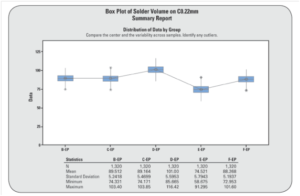 Figure 5. Box plot of solder volume on a C0.22mm pad (EP stencil).
 Figure 6. Box plot of solder volume on a C0.22mm pad (nanostencil).
Box Plot of EP and Nanostencil on a SQ0.20mm Pad
A similar trend was observed in the SQ0.20mm box plot result (Figures 7 and 8), where stencil D had the highest mean value for both the EP and nanostencil at 101.76% (EP) and 110.78% (nanostencil). EP stencils C and D had the lowest solder volume variation with a comparable standard deviation while nanostencil A had the lowest volume variation with a standard deviation of 3.8574.
 Figure 7. Box plot of solder volume on a SQ0.20mm pad (EP stencil).
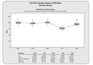 Figure 8. Box plot of solder volume on a SQ0.20mm pad (nanostencil).
Process Capability Analysis
Further analysis was performed to measure the Cpk and Cp of each stencil. The specification limit was set at a default of 60% for LCL and 150% for UCL to give a better comparison of Cpk and Cp between different stencils. Cpk is used to define the accuracy and consistency of the paste transfer efficiency. In the case where the process is not centered but still within the upper and lower spec, Cp value is used to define the process consistency. Based on results shown in Table 3, stencil D had the highest Cpk value on a C0.20mm pad for both the EP stencil and nanostencil. It showed that stencil D was able to achieve consistent solder volume with a mean closest to the target value. Out of the stencils available, EP stencil E performed poorly on transfer efficiency where a number of pads achieved volume below the lower spec limit of 60% (Figure 9). There are various factors that potentially contributed to the poor transfer, which are not the focus in this study. Despite differences in the Cpk value, nanostencils improved consistency of transfer efficiency as all stencils achieved a comparable Cp value of more than 3.
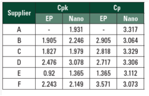 Table 3. Capability analysis of stencils on C0.22mm.
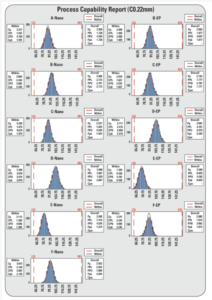 Figure 9. Cpk report of stencils on C0.22mm
For the SQ0.20mm pad, stencil D achieved the highest Cpk on EP, but nanostencil F had the highest Cpk value, as seen in Table 4. One of the possible reasons for this is that the data distribution of stencil D is not centered, which can be reflected within the box plot analysis where stencil D achieved a mean solder paste volume of 110.78%. Most stencils with a nanocoating provided better consistency as reflected in the Cp value >3 for all nanostencils (Figure 10).
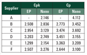 Table 3. Capability analysis of stencils on C0.22mm.
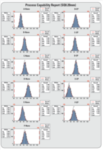 Figure 10. Cpk report of stencils on SQ0.20mm.
One-Way ANOVA Analysis
In order to assess the mean value differences between stencils statistically among suppliers, one-way ANOVA analysis was performed on both C0.22mm and SQ0.22mm data:
Null hypothesis, H0: All means are equal
Alternative hypothesis, H1: At least one mean is different
C0.22mm Pad
The results of both EP and nanostencils show that p-value < 0.05 indicate that the data provides sufficient evidence to reject the null hypothesis that at least one mean is different among EP and nanostencils (Figures 11 and 12). Further analysis performed using Tukey Pairwise comparison shows that all EP stencils have significant mean differences except for EP stencils B and C, while all nanostencils have significant differences between them (Figure 13 and 14).
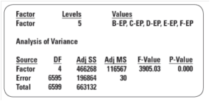 Figure 11. One-way ANOVA analysis results on a C0.22mm pad (EP stencil).
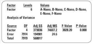 Figure 12. One-way ANOVA analysis results on a C0.22mm pad (nanostencil).
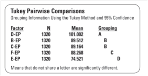 Figure 13. Example of Tukey Pairwise Comparisons (EP stencil).
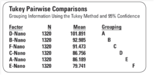 Figure 14. Example of Tukey Pairwise Comparisons (nanostencil).
SQ0.20mm Pad
The results of both EP and nanostencils show that p-value <0.05 indicate that there is sufficient data evidence to reject the null hypothesis and at least one mean is different among EP and nanostencils. Similarly, further analysis performed using Tukey Pairwise comparison shows all EP stencils are significantly different from one another. Nanostencil C and stencil F do not show a significant difference.
Impact of Nanocoated Stencil Helps with Transfer Efficiency
Several published papers show different opinions on the impact of nanocoated stencils regarding printing transfer efficiency. Based on the results of this study, most nanostencils provided a slight improvement in transfer efficiency and less volume variation, as shown in the box plot and capabilities analysis. Varied results obtained in different published papers could be a result of different nanomaterials used and different methods that nanomaterial was applied to the stencils.
Impact of Printing Performance on 0.18mm Circle and Square Shapes
While it is not the scope of this study to focus on the 0.18mm pad, the box plot results in Figure 15 indicate the differences in printing performances of each stencil when the area ratio is reduced to 0.59. A significant difference in transfer efficiency and variation was observed among different stencil suppliers.
In a similar pad size, square-shaped pads have a better transfer efficiency compared to circle pads. However, more data needs to be collected in order to make a conclusion regarding the observation.
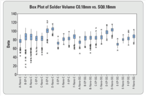 Figure 15. Box plot of solder volume C0.18mm vs. SQ0.18mm.
Conclusion
The following is the summary from this study:
- All EP and nanostencils, except for stencil E, were able to perform good printing performance with Cpk >1.67 on SQ0.20mm and C0.22mm pad.
- With a C0.22mm pad, stencil D achieved high transfer efficiency on the EP and nanostencil. One-way ANOVA analysis showed that there was a significant mean difference on EP stencils, except for stencils B and C, while all nanostencils had significant differences with each stencil.
- With the SQ0.20mm pad, stencil D achieved high transfer efficiency on the EP stencil and stencil F on nanostencil. One-way ANOVA analysis showed that all EP stencils were significantly different from one another, while only nanostencils C and F were not significantly different.
- Nanocoated stencils improved slightly on transfer efficiency and provided lesser volume variation.
Based on this study, we can conclude that different stencils will provide different printing performances. There are a few possibilities that could contribute to the differences, such as the accuracy of laser cutting aperture dimensions, consistency of foil thickness, smoothness of the aperture side wall, nanomaterial, and the method by which the nanocoating material is applied. Verification of the factors are beyond the scope of this study, and will be part of the consideration for future work.
Future Work
We are following up this study with an assessment study on factors that contribute to the differences between stencils, and the impact that stencil foil materials such as fine-grain, semi-fine grain, and standard stainless steel SUS304 have on printing performance.
References
- Kenneth Thum, Jonas Sjoberg, Sze Pei Lim, “Printing Capability Study of 008004 (0201m) Components for SiP Applications,” SMTA SEA 2014.
- Rita Mohanty, PhD., S. Manian Ramkumar, PhD, CEMA, Chris Anglin, Toshitake Oda, “Effect of Nanocoat Stencil on 01005 Printing,” APEX 2011.
- Whittier, R. and Shea, C., “Evaluation of Stencil Materials, Suppliers, and Coatings,” Proceedings of SMTA International Conference, September 2011.
- Farrell, R. and Shea, C., “Stencil and Solder Paste Inspection Evaluation for Miniaturized Components,” Proceedings of SMTA International Conference, September 2014.
Authors
Jeffrey Len is a technical support engineer for Indium Corporation and is based in Penang, Malaysia. He is responsible for providing comprehensive technical advice in the selection, use, and application of Indium Corporation’s entire range of products to customers in northern Malaysia. Len’s previous experience includes improving processes to increase output quality, and developing customer relationships to better service individual needs. Len holds a bachelor’s degree in pure chemistry from Universti Sains Malaysia in Penang, Malaysia.
LEON RAO
 Leon Rao is Senior Technical Support Engineer for Indium Corporation’s customers in Eastern China and is based in Suzhou, China.
Leon is responsible for providing comprehensive technical advice in the selection, use, and application of Indium Corporation’s entire range of products to customers in the Shanghai and Hangzhou area.
Leon joined Indium Corporation in 2013 as a Technical Support Engineer. He has extensive experience providing on-site support for new product evaluations, product selection, and troubleshooting. Leon earned his bachelor’s degree in Applied Physics from the Jingdezhen Ceramic Institute.
EVAN YIN
 Evan Yin is the assistant manager at Indium Corporation’s Suzhou Process Simulation Lab, and is responsible for equipment engineering. He provides technical support and services, such as product and process recommendations, troubleshooting, and conducting product evaluations and qualifications.
Before joining Indium Corporation in 2017, Yin worked in the surface mount technology field for more than 15 years. He has a degree in computer information management from Soochow University.
WISDOM QU
 Wisdom Qu is Area Technical Manager, Eastern China. She provides technical support for Indium Corporation’s electronics assembly materials, semiconductor and advanced assembly materials, and epoxy flux products. She is based in Suzhou, PRC.
Wisdom has over nine years of experience in surface mount technology and has been a technical support engineer with Indium Corporation since 2005. In 2007, she was recognized by Indium Corporation for her expertise with the Silver Quill Award for Best Paper/Presentation of the year. Wisdom has presented at several technical conferences and customer sites.
Wisdom has a degree in mathematics from Hubei Radio and Television University in China. She is an SMTA Certified Process Engineer.


