This article highlights the challenges faced during SoC assembly with both commercial EDA tools and internal tools or scripts and also describes a solution to handle the state-of-art SoC designs.
In recent years, new inflection points have surfaced in the creation and delivery of system-on-chip (SoC) designs to address the fast moving consumer markets like mobile, tablets, home entertainment, graphics, gaming, internet of things (IoT) and infotainment.
Some of the inflection points are:
- Concurrent design implementation with early IP level RTL creation and SoC assembly
- Low power requirements driving the need for many power domains, requiring upfront architectural decisions, as well as RTL modifications to suit downstream implementation
- Adoption of many third-party IPs (e.g., 32/64 bit ARM architectures, Imagination PowerVR IP)
- Network on Chip (NoC)/Bus Fabric usage
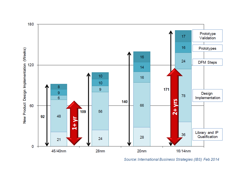
Figure 1 below shows the SoC productivity cycle challenges for the newer technology nodes. The estimated IP qualification and design implementation time has doubled to around two years from 45nm to 16nm, which requires a significant improvement in productivity.
This article highlights the challenges faced during SoC assembly with both commercial EDA tools and internal tools or scripts and also describes a solution to handle the state-of-art SoC designs.
SoC Productivity Challenge
Some of the SoC assembly challenges with the existing solutions:
- Tools/scripts do not handle the latest RTL language constructs
- Tools/scripts do not scale to handle large SoCs with 1000s of IPs and millions of nets
- Tools/scripts do not allow grouping/ungrouping/moving instances or creating IP clones or rerouting 1000s of nets across hierarchies with behavioral RTL
- Tools/scripts do not generate friendly RTL for downstream power intent aware synthesis flows
- Tools/scripts have limited capability for porting an existing ASIC design to multiple FPGAs for prototyping
- Commercial tools have limitations in combining RTL views and IP-XACT standard interface views for chip assembly
One of the major challenges during design implementation is to quickly assemble the SoC, verify it, and take it through synthesis and floorplanning to get an estimate of timing and die area. SoC assembly tools don’t scale to handle today’s complex designs and register transfer language requirements (e.g., SystemVerilog interfaces). Majority of the users have developed homegrown tools for chip assembly and these tools or scripts need constant maintenance for every new project and provide limited automation for dispersed teams. Another challenge with current SoC assembly tools is the lack of automation for RTL design modifications and restructuring to accommodate for physical design changes to meet area, timing and power requirements. RTL restructuring is needed to minimize iterations during the physical design process for new revisions of the design and making sure that the physical synthesis step takes into consideration the changes made to meet the timing, congestion or power requirements. The restructuring of RTL is a risky, manual and error prone process and manual editing takes three to four weeks for each revision of the design.
A new application area of automated assembly and design modification at RTL is for FPGA prototyping to split the large ASIC RTL into multiple FPGAs while making changes to the clocking and DFT logic. FPGA prototyping is also a manual task and requires -three to four weeks in modifying the design.
SoC & IP Sub-system Assembly Requirements
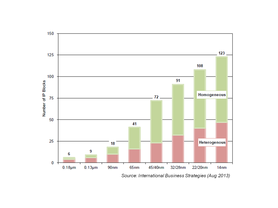
Today’s SoC may contain 100 or more IPs (including top-level glue or integration logic), many of which may have 100 or more ports. Figure 2 below shows the number of homogenous and heterogeneous IP blocks in the current technology nodes. The number of IP blocks per design includes both homogeneous and heterogeneous IP blocks. The use of pre-designed IP blocks to reduce the complexity of system integration has gained popularity lately. Using pre-designed IP blocks leads to the reduction of time and complexity of system level design. Heterogeneous IP blocks are provided by different vendors, and differ in their interfaces. In order to improve design reuse, methods for combining heterogeneous IP blocks with incompatible protocols and I/Os are needed.
The RTL sub-systems received from third-party configurable IP vendors like ARM or Imagination also have many challenges. Some of them are:
- The RTL received have complex usage of Verilog pre-processors (`ifdef, `include etc)
- The RTL received is hierarchical with complex usage of RTL constructs
- Frequent RTL drops are created for some of these IPs which needs automation
The requirements from end users of configurable third-party IP are:
- Make changes to the IPs for larger or smaller buses
- Update the IPs (e.g., memories) with internal library components
- Insert logic (e.g., DFT or power management) in these sub-systems
- Sub-system assembly required with other IPs to create a new sub-system
- Hierarchy manipulation of some sub-systems needed
- Assembly tool needs to support some IPs in IP-XACT format while the configurable IP is in RTL format
- Create IP-XACT views of the sub-systems in addition to hardening the RTL for end delivery to SoC groups
Designers have already realized that creating, reviewing and maintaining over 100,000 connections in a high level design language (HDL) through a text editor would be exceptionally painful. Many have moved to an eminently logical solution, i.e., capture the connections in a spreadsheet (e.g., MS Excel), then write a script to convert from that spreadsheet to a Verilog or VHDL netlist. However, spreadsheet-based solutions have a limitation in that they do not scale well across the needs of multiple design groups within an organization.
Building connectivity with scripts at RTL has its liabilities, the primary one being that users cannot use interfaces and interface connections. However, in order to manage complexity, designers absolutely need to be able to do so with minimal manual connectivity effort. Since each interface encapsulates a significant number of signals (for example an AXI bus), making connections through interfaces reduces the total number of connections by as much as 95%. Achieving this goal depends on heavy use of interfaces, rather than ad-hoc ports on components.
The Atrenta Solution – GenSys® for Automated SoC Assembly and RTL Restructuring
Atrenta’s GenSys solution has been developed with leading semiconductor companies servicing the consumer market. The goal of this work has been to reduce front-end development effort for SoC platforms and derivative designs by more than an order of magnitude, while also dramatically reducing the level of human error in assembly. To accomplish these goals, Atrenta has developed a product which fully supports architectural planning and a programmed handoff to back-end design. A well-documented methodology is part of GenSys. Many industry standards, including IP-XACT are supported.
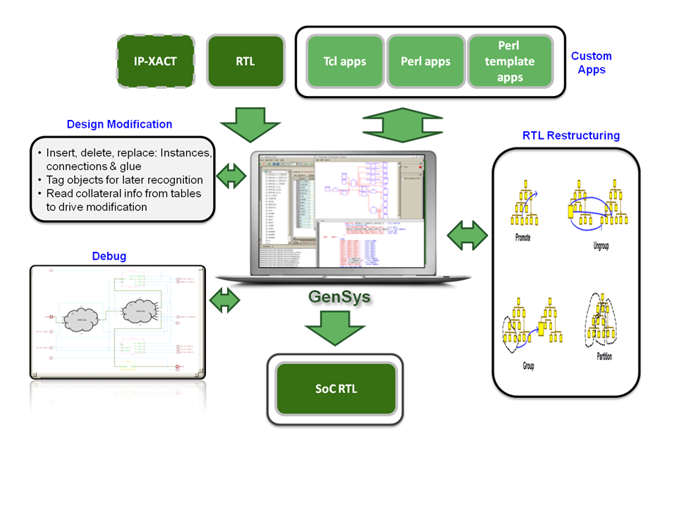
Figure 3 above shows the various capabilities of GenSys to take in different RTL blocks along with interface views of IPs in the IP-XACT standard. The solution supports:
- Fully interoperable (import and export) with several standards including IP-XACT, Verilog, SystemVerilog and VHDL (both designs and components), CSV and Tcl
- Support for a bottom-up design methodology through standard hierarchical methods and a top-down design methodology through the ability to change hierarchy on the fly, and create/edit new components in place
- Comprehensive connectivity checking with sort/filter options to review how and why connections are made, and a direct connection to Atrenta’s SpyGlass® suite for a broad range of RTL design analysis
- Interface-based connectivity reduces user-defined connections by 95% or more. Ad-hoc connectivity is also supported through a high-productivity interface
- Support of a comprehensive set of connection techniques with splices and overrides to handle permanent and temporary tie-offs and opens, handling all the special cases that happen in real designs
- User-definable auto-connect techniques aid completion of many connections
- Preserve configurability in any form (parameters, `define, `ifdef) in generated RTL
- Tcl scripting, advanced GUI & replay
The GenSys RTL restructuring capabilities include:
- Restructuring and mapping of existing RTL to a new application due to physical or power management requirements
- Re-partitioning the design to reduce placement instances to the limits of the physical design tool
- Insertion of power management or test logic in synthesizable IP blocks (third-party and internal)
- Insertion of feed-throughs to accommodate rerouting of nets to minimize wire length during physical implementation
Summary
Today’s SoC need state-of-the-art solutions to handle design complexity and HDL constructs. The overall benefits seen by SoC integration architects and engineers using GenSys are that the solution builds “correct-by-construction” chip and sub-system assemblies, reducing time to capture and debug,showing immediate turnaround time for capture and edit of full-chip designs. The solution helps dispersed design teams to create more consistent, high-quality designs by exploiting the full power of effective design re-use and IP integration.
The GenSys solution integrates seamlessly into existing design environments, dramatically enhancing efficiency of installed tools and methodologies and is silicon proven on multiple designs. Customers have seen over 20x reduction in chip/sub-system assembly effort over traditional methods.
____________________________________________________________________________________
About Author
Kiran Vittal, Sr. Director with Atrenta Inc. Kiran can be reached on kvittal@atrenta.com


