Wei Chen, Peter Guan, and David Chen, Analog Devices
The increasing demand for computing power in notebook computers has driven up CPU clock frequency and supply currents significantly. Meanwhile, supply voltages have quickly decreased as CPUs migrated to finer line-width processes. As the CPU clock frequency exceeds 1GHz, the core supply current has for the first time surpassed 20A and the minimum supply voltage has dropped below 1V. Most of the forthcoming mobile CPUs call for core supply currents as high as 25A. In some cases, the supply current could exceed 30A. The Intel Mobile Voltage Positioning (IMVP) specs have been enacted to deal with these new mobile processor power requirements.
Linear Technology’s new LTC3714 and LTC3716 controllers are designed to comply with the IMVP specifications. The LTC3714 is a constant on-time, No RSENSE™, current mode controller, intended for mobility-oriented portable computer applications. The LTC3716 is a dual-phase current mode controller intended for performance-oriented portable computer applications.
The IMVP2 specs require three digital signals in addition to the 5 VID bits to command different operation modes: battery optimized mode (BOM), performance optimized mode (POM), deep sleep mode (DPSLP) and deeper sleep mode (DPRSLP). Under the BOM, DPSLP and DPRSLP modes, the output voltage is reduced to conserve the battery energy. IMVP also calls for voltage positioning techniques to minimize the number of output capacitors while maintaining a tight output regulation during large and fast load transients. Both the LTC3714 and LTC3716 can implement active voltage positioning techniques (AVP) without suffering additional power loss as they would with the conventional passive droop technique.
Single-Phase vs Dual-Phase
The traditional single-phase solution uses a single synchronous buck circuit to convert the high voltage battery or adapter input (as high as 21V) to a low voltage (0.7V–1.8V) CPU core supply. This solution relies on paralleling several MOSFETs and using a bulky inductor to deliver the required high currents. However, when a high voltage is input to the circuit, most of the single-phase MOSFET drivers are not strong enough to efficiently drive several paralleled, high current MOSFETs without dV/dt shoot-through problems. The resulting excessive power loss in MOSFETs increases the thermal stress near the CPU and reduces battery run time. More importantly, frequent dV/dt shoot-through can cause catastrophic failure in MOSFETs. If the top MOSFET fails by shorting the drain to source, the high input voltage will be applied directly to the CPU, destroying the system.
Using a higher switching frequency increases load transient response speed, but it also yields lower efficiency and places higher thermal stress on the power supply. The maximum input ripple current in the single-phase circuit is about 30%–50% of the output load current. At an output current of 25A, the input ripple current for the core power supply will be about 8ARMS. The large input capacitors required increase both the size and cost of the power supply. If not properly filtered, this ripple current will decrease the battery run time. Additionally, the physical height of a high current (25A) inductor becomes unacceptably large and additional low ESR output capacitors are required to handle load current steps. Current crowding in the PCB traces near the inductor pads raises reliability concerns. As a result, the single-phase solution is not only inefficient and bulky, but causes long-term reliability problems. Based upon present power component technology, single-phase solutions are not viable if the CPU supply current exceeds 20A. A 2-phase configuration is a superior alternative in this application.
A dual-phase architecture parallels two synchronous buck stages to provide a single high current output. The clocks of the two buck stages are interleaved 180 degrees out of phase, resulting in ripple current cancellation at both the input and output terminals of the power supply. The resulting input ripple current reduction significantly decreases the input capacitor size and improves battery life. Also, because of the output ripple current cancellation, lower value inductors can be used. These two smaller inductors are effectively in parallel during the load transients. Accordingly, much faster load transient response and current slew rate are achieved without increasing the switching frequency. This helps obtain high power-conversion efficiency to maximize battery run time and to reduce the thermal stress near the CPU. Because current is divided equally between two identical channels, the heat is distributed uniformly and the long-term PCB reliability is enhanced. Since each inductor carries only one-half of the total current, the height requirement of each inductor is significantly reduced. With proper design optimization, a higher efficiency, lower profile and lower cost solution can be achieved with the 2-phase architecture.
LTC3714 Single-Phase IMVP Solution
The LTC3714 is designed to power mobility-oriented notebook CPUs. The constant on-time architecture of the LTC3714 and its wide input voltage range of 4V to 36V allow one-step regulation from the battery source to the processor’s core voltage. Its programmable frequency of up to 1MHz also allows designers to choose smaller inductors and capacitors for high frequency operation. For high power operations, a lower frequency can be programmed, improving efficiency and reducing MOSFET heat dissipation. True current mode sensing ensures that current is controlled during every cycle, which results in excellent line and load regulation. Internal power MOSFET drivers are capable of efficiently driving three power MOSFETs in parallel, saving the cost and space of a separate MOSFET driver IC.
The LTC3714 also has many features, such as internal foldback current limiting, output overvoltage comparator, soft start, and an optional short-circuit shutdown timer. Five VID input bits program the output in steps of 50mV or 25mV from 0.6V to 1.75V.
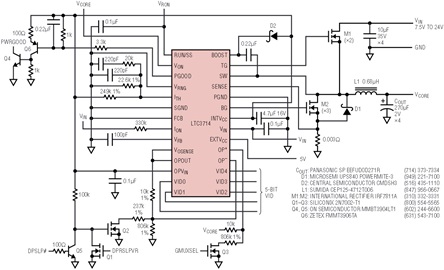
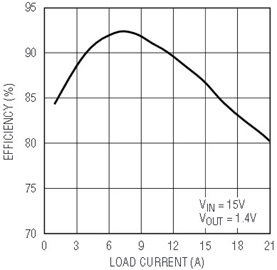
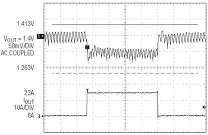
Figure 1 shows the complete schematic diagram using the LTC3714 for CPU currents of up to 20A. The design uses only five SO-8 FETs (IRF7811A), one low profile inductor and 4 SP caps at the output. Small-signal transistors Q1–Q3 and Q5 are used with the internal op amp of the LTC3714 to enable different power-saving options. Q4 and Q6 are used to filter glitches shorter that 100µs during mode transitions. Figure 2 shows the test results for efficiency and load transient response. Greater than 80% efficiency is maintained over the load range of 2A to 21A with an output of 1.40V. Because of AVP, the output voltage variations are less than 100mVP-P when the load current steps between 8A and 23A.
LTC3716 Dual-Phase IMVP Solution
The LTC3716 is intended for performance-based IMVP applications requiring CPU currents of 20A to 40A. It is available in a small, low profile, narrow SSOP, 36-pin package. Each controller can drive two synchronous buck circuits 180 degree out of phase. True peak current mode control is employed to ensure good current sharing between the paralleled buck stages. Four high current N-MOSFET drivers are integrated into the controller to minimize the overall size of the power supply. Anti-shoot-through circuitry prevents the top and bottom FETs from conducting simultaneously. The LTC3716 also provides a rich array of features, such as a PGOOD signal, soft-start, overvoltage protection, foldback current limit, and defeatable overcurrent latch-off. The part features discontinuous conduction and Burst Mode™ operation for light loads, to minimize power loss when the CPU is in sleep mode. These features make the device particularly attractive for mobile computing applications.
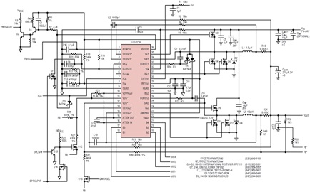
Figure 3 shows a complete schematic diagram of a 25A dual-phase mobile CPU core power supply. With only one IC, six tiny SO-8 MOSFETs (IRF7811A) and two 1µH low profile, surface mount inductors, an efficiency of about 82% is achieved for a 15V input and a 1.40V/25A output. Greater than 80% efficiency can be maintained throughout the load range of 2A to 25A. Q12–Q14 and Q16 are used with the internal op amp to select different power-saving options.
Figures 4a and 4b show the measured efficiency and load transient responses, respectively for Figure 3’s circuit. With only three SP caps, the circuit can meet IMVP2 output regulation spec for a 15A load step: the output voltage changes from 1.383V to 1.273V when the load current changes from 8A to 23A.
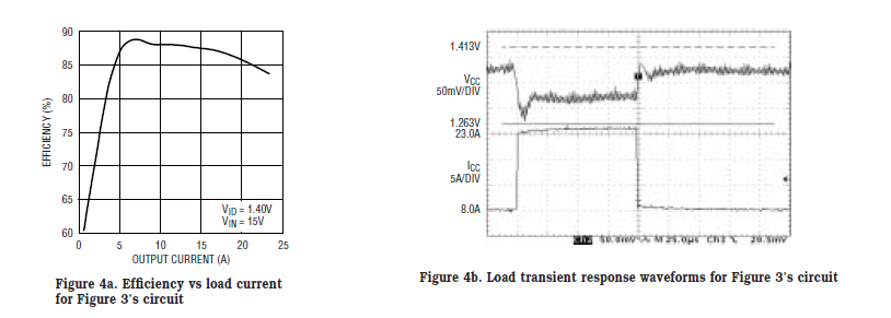
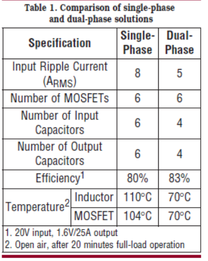
Table 1 compares the performance of key aspects of single-phase and dual-phase designs for a 20V input and 1.6V, 25A output. The dual-phase technique saves two output capacitors (270µF/2V, SP capacitors) and two input capacitors (10µF/35V, Y5V). With the same number of MOSFETs (IRF7811A) and the same switching frequency, the dual-phase solution achieves higher efficiencies. The higher efficiency of the dual-phase circuit, coupled with more uniform current distribution, dramatically reduces the temperature rise in both the MOSFETs and the inductors.
Conclusion
The new IMVP spec calls for a power supply design that minimizes power loss under different operational modes. The LTC3714- and LTC3716-based solutions are able to satisfy the specs with a minimum cost increase. Whereas the LTC3714 is suitable for mobility-oriented notebook computers, the LTC3716 provides the optimum power solution for performance-based notebook computers because it achieves high efficiency, small size and low solution cost simultaneously. Compared to a conventional single-phase solution, the dual-phase solution reduces input and output capacitors, minimizes power losses, increases the battery run time and improves long term PCB reliability. Since CPU current requirement continues to increase, the dual-phase solution will satisfy the power requirements for several future generations of mobile CPUs. Furthermore, the adoption of a dual-phase solution will reduce the likelihood of having to redesign the power supply for higher frequency CPUs over the next three to four years.


