Graphene material much interest for researches as proven to be superior for future applications. IBM has most recently proven that graphene is optimally suited for radio frequency and wireless communications. This could be huge. . The most applicable uses of graphene so far are those for solar cells and batteries.
Silicon and carbon fiber are still the main resources utilized within the hardware industry but both could be replaced by this industry altering nanomaterial. However, there are still fundamental issues related to reasonable manufacturing costs, production efficiency, and technical implementation that continue to hold graphene in the test tube.
IBM first succeeded at using graphene in electronics in 2011 with their circuit board integration. Now, they have proven that the material can effectively be used to perform modern methods of communication that we most often undertake with mobile devices. The IBM research blog reports they have now created:
“…the world’s most advanced, fully functional integrated circuit made of wafer-scale graphene – 10,000 times better performance than previously reported efforts.”
It seems that those most knowledgeable on the subject predict that graphene’s first implementation in the consumer market will come in the form of sensors. That prediction is probably correct, according to IBM:
“Integrating graphene radio frequency (RF) devices into today’s low-cost silicon technology could also be a way to enable pervasive wireless communications allowing such things as smart sensors and RFID tags to send data signals at significant distances.” 
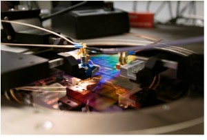
A wafer of graphene chips, being tested at IBM Research
Circuits built on graphene could allow mobile devices – tablets to wearables – to transmit data much faster, in a more cost-effective manner, than today’s silicon-based chips. For example, the circuits we built for wireless receivers consume less than 20 mW power to operate, while also demonstrating the highest conversion gain of any graphene RF circuits at multiple GHz frequency – successfully receiving and restoring a digital text message (“I-B-M”) carried on a 4.3 GHz signal without any distortion.
IBM’s circuit consists of three graphene transistors, four inductors, two capacitors, and two resistors. All circuit components are fully integrated into a 0.6 mm2 area and fabricated in a 200 mm silicon production line. The researchers say that those the circuits consume less than 20 mW power to operate, while also demonstrating the highest conversion gain of any graphene RF circuits at multiple GHz frequency.
IBM already built an analog graphene integrated circuit with a broadband frequency mixer in a 2011, but that device suffered from poor performance due to harsh fabrication processes. For this new IC, the research team completely reversed the conventional silicon integrated circuit fabrication flow, leaving graphene transistors as the last step of integrated circuit fabrication. This resulted in preserving graphene device performance.


