
Layered semiconducting black arsenic phosphorus as an alternative to silicon
 Graphene, the only one atom thick carbon network, achieved overnight fame with the 2010 Nobel Prize. But now comes competition: Such layers can also be formed by black phosphorous. Chemists at the Technical University of Munich (TUM) have now developed a semiconducting material in which individual phosphorus atoms are replaced by arsenic. In a collaborative international effort, American colleagues have built the first field-effect transistors from the new material.

For many decades silicon has formed the basis of modern electronics. To date silicon technology could provide ever tinier transistors for smaller and smaller devices. But the size of silicon transistors is reaching its physical limit. Also, consumers would like to have flexible devices, devices that can be incorporated into clothing and the likes. However, silicon is hard and brittle. All this has triggered a race for new materials that might one day replace silicon.
Black arsenic phosphorus might be such a material. Like graphene, which consists of a single layer of carbon atoms, it forms extremely thin layers. The array of possible applications ranges from transistors and sensors to mechanically flexible semiconductor devices. Unlike graphene, whose electronic properties are similar to those of metals, black arsenic phosphorus behaves like a semiconductor.
Phosphorene vs. graphene
A cooperation between the Technical University of Munich and the University of Regensburg on the German side and the University of Southern California (USC) and Yale University in the United States has now, for the first time, produced a field effect transistor made of black arsenic phosphorus.
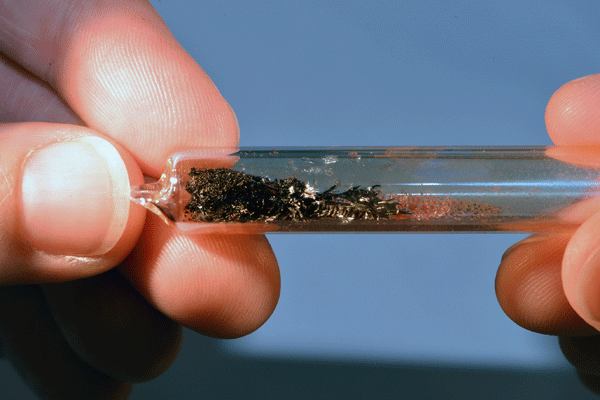
The compounds were synthesized by Marianne Koepf at the laboratory of the research group for Synthesis and Characterization of Innovative Materials at the TUM. The field effect transistors were built and characterized by a group headed by Professor Zhou and Dr. Liu at the Department of Electrical Engineering at USC.
The new technology developed at TUM allows the synthesis of black arsenic phosphorus without high pressure. This requires less energy and is cheaper. The gap between valence and conduction bands can be precisely tuned by adjusting the arsenic concentration. “This allows us to produce materials with previously unattainable electronic and optical properties in an energy window that was hitherto inaccessible,” says Professor Tom Nilges, head of the research group for Synthesis and Characterization of Innovative Materials.
Detectors for infrared
With an arsenic concentration of 83 percent the material exhibits an extremely small band gap of only 0.15 electron volts, making it predestined for sensors which can detect long wavelength infrared radiation. LiDAR (Light Detection and Ranging) sensors operate in this wavelength range, for example. They are used, among other things, as distance sensors in automobiles. Another application is the measurement of dust particles and trace gases in environmental monitoring.
A further interesting aspect of these new, two-dimensional semiconductors is their anisotropic electronic and optical behavior. The material exhibits different characteristics along the x- and y-axes in the same plane. To produce graphene like films the material can be peeled off in ultra thin layers. The thinnest films obtained so far are only two atomic layers thick.
This work was supported by the Office of Naval Research (ONR), the Air Force Office of Scientific Research (AFOSR), the Center of Excellence for Nanotechnologies (CEGN) of King Abdul-Aziz City for Science and Technology (KACST), the German Research Council (DFG) and the TUM Graduate School.


