
Current can literally blow copper interconnects away, but graphene could keep them intact
Most of the hand-wringing over the fate of Moore’s Law focuses on the ever-shrinking silicon transistor. But increasingly researchers are concerned with another critical part of the infrastructure: the copper wires that connect individual transistors to form complex circuits.
At the IEEE International Electron Devices Meeting in San Francisco in December, researchers described the coming problems for copper interconnects and debated ways of getting around them. One approach, studied by a group led by Stanford electrical engineer H.-S. Philip Wong, is to gird copper with graphene. Wong’s group found that the nanomaterial can alleviate a major problem facing copper, called electromigration.
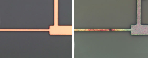
Copper wires are getting so thin, and must carry so much current, that the atoms in the wire can literally get blown out of place. “The electron wind can physically move the copper atoms and create a void,” says Wong. Growing graphene around copper wires prevents this, according to research that Wong’s group presented at the meeting. It also seems to bring down the resistance of the copper wires.
Ruth Brain, an Intel Fellow and director of interconnect technology and integration at the company’s Hillsboro, Ore., location, explained how interconnects are being pushed to their limits. More transistors per chip area means more interconnects have been installed to connect them. The first chips to use copper interconnects, which were produced in 2000, had 1 kilometer of wiring per square centimeter. Today’s 14-nanometer-node processors contain more than 10 km of copper wiring in the same area, she said.
In order to improve performance, the ever-narrowing copper wires must carry ever more current. The amount of current per area in a wire is called its current density, which has been increasing on cutting-edge chips for two reasons: Wires are shrinking, and higher currents must course through them to enable the faster switching speeds that boost performance.
And herein lies the challenge: The narrower the wire, the higher its resistance. “Interconnects have had to shrink while increasing the current densities by 20 times,” said Brain. “You would burn your house down if you did this in your house.”
Today’s solution is to deposit copper interconnects within trenches lined with 2-nanometer-thick walls of tantalum nitride. This lining keeps the copper from escaping, and Wong says copper will probably endure through the coming 10- and 7-nm nodes. As device features keep shrinking, though, 2-nm walls will be far too thick, says Wong. Researchers are investigating other linings that may prevent electromigration, including ruthenium and magnesium, but at 0.3 nm, he says, graphene is thinner than anything else.
The semiconductor industry avoids integrating new materials as long as possible, but Wong says there isn’t much choice in this situation: If copper’s life can’t be extended, it will have to be replaced with a new material anyway, such as cobalt.
The Stanford group worked with Lam Research Corp., which makes chip manufacturing tools, as well as researchers from Zhejiang University, in China, to make and test the composite interconnects. The materials make a good pair; graphene is often made by growing it on copper. Lam Research has developed a proprietary process for doing this at temperatures that won’t damage the rest of the chip—below 400 °C. Compared to copper alone, the composite limited electromigration by a factor of 10. And the composite wires had half the electrical resistance.
Wong says the interconnect problem can no longer be dismissed. “Before, most of the time we were hearing about transistors,” he says. “Now it’s not just transistors but wires, memory—many other things that were previously not a problem are beginning to be a problem.”


