 Power management is a well-known and understood aspect of product development, but just as with everything else in the electronics industry, it must evolve with new demands for efficiency.
Part of the drive for connecting electronic products on the scale of the Internet of Things is that with greater connectivity comes greater control. While that can mean different things to different people, there is high expectation that the IoT will bring greater control over the way power is used. This sits well with the globally accepted impetus to deliver energy savings by making products more energy efficient in general, exemplified by the G20 Energy Efficiency Action Plan.
Regional legislation is already in place across Europe to enforce compliance with targets for 2020 (which includes a 20% improvement in energy efficiency), with more laws and regulations being developed. This puts pressure on OEMs to comply with the new standards for power efficiency, which, in turn, is driving innovation from semiconductor manufacturers.
There is an opportunity for the IoT to play a crucial role in meeting these targets, by enabling greater control over energy use. This could range from a Building Management System autonomously controlling the HVAC of a large building based on occupancy, to allowing homeowners to moderate their heating and lighting remotely using a smart device. Conceptually the same principle can be applied to equipment such as servers that may spend at least some of their uptime in between performing useful tasks. Just as Stop-Start technology is now being used in vehicles, the same approach can be used in electronic equipment to deliver cumulatively significant savings.
In the European Union, the Energy Efficiency Directive will likely cover many of the products that will form part of the ‘I’ in IoT; the millions of switches and servers that will effectively provide the connectivity between all of the (billions) of nodes. While there isn’t (currently) any legislation that applies explicitly to the actual nodes that will sit on the edge of the IoT, there is legislation covering the amount of power that mains-powered products are permitted to use in ‘standby’ and ‘off’ modes, which was joined more recently by legislation covering similar products that are networked (The Energy Efficiency Directive 2012/27/EU Lot 6 and Lot 26 respectively). This implies that as devices get ‘smarter’ in the way they work, they must also get smarter about how they rest.
A new paradigm for power
The power density paradigm that hit the semiconductor industry in the early years of this century caused a massive shift in the way integrated devices were designed, particularly digital devices based on CMOS processes. Efforts to reduce active power in microprocessors were driven by the amount of heat that could be dissipated at the transistor junction. As a result, modern devices all feature low power modes of operation. These will be drawn upon to enable the IoT, particularly in devices that are battery powered or, possibly, use energy harvested from their operating environment.
However, it remains likely that many more devices will be powered either directly or indirectly from the mains power network. Power conversion has always been an area where small improvements in conversion efficiency can add up to big savings in running costs. With the advent of energy regulation, it is no more a case of reducing the operational costs of large equipment, but minimising the energy demand of everyday devices, including white goods around the home.
Converting power from a high voltage AC source to a series of low voltage DC supplies incurs inherent losses, but the loss that can occur at the inlet is one that involves no conversion. Instead, the passive components on the supply used to provide a safe discharge path also present a leakage path that, unless physically disconnected, will always be present. In the past, this may have been seen as an unavoidable loss, but a device from Power Integrations effectively reduces those losses to zero.
The CAP200DG in the CAPZero-2 family sits across the AC supply (see Figure 1) and blocks current flow in the X capacitor safety discharge resistors (R1 and R2) during normal operation. This reduces the power loss to less than 5mW or, as IEC 62301 clause 4.5 rounds down standby power that is below 5mW to zero, it removes the loss completely at 230VAC.
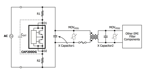
When the AC voltage is removed, the path through the resistors is re-established, allowing the X capacitor to be fully discharged, even below published SELV (safety extra low voltage) values. This means the CAP200DG Zero Loss Automatic X Capacitor Discharge IC can also be used in applications where the input voltage is as low as 18VAC.
Exceeding legislation
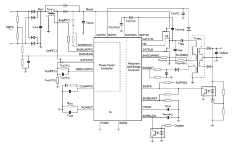
Achieving less than 0.5W in standby mode, as defined by EuP Lot 6, is now aided by a range of power controllers from leading suppliers. Typically, these will integrate Power Factor Correction (PFC) and may include other features. An example is the TEA1716T from NXP, a resonant power supply controller with PFC; implemented as a multi-chip IC that also integrates a Half-Bridge resonant Converter (HBC). The device can drive a discrete MOSFET in an up-converter and two discrete power MOSFETs in a resonant half-bridge configuration.
It targets power supplies delivering between 90W and 500W from a mains supply ranging from 70VAC to 276VAC. It requires few external components and can be designed to operate in a standalone mode or with an external DC source.
Both the PFC and HBC controllers in the TEA1716T have been designed to operate in burst mode, in which the controllers are first ‘on’ for a period and then ‘off’ for a period. Burst mode can increase the efficiency of a power supply under low-load conditions.
The HBC circuit converts the 400V boost voltage from the PFC into one or more regulated DC output voltages, as well as driving the external MOSFETs. A transformer, exhibiting both leakage inductance and magnetising inductance, forms part of the resonant circuit, along with a resonant capacitor and the load at the output. The external MOSFETs driven by the HBC circuit are connected to the resonant circuit in the half-bridge configuration.
The device employs an advanced adaptive non-overlap timing method, which delivers higher switching efficiency, helping the device meet the EuP Lot6 specification. It also guarantees safe switching even under fault conditions. Other safety features include High Frequency Protection, which protects from the effects of a disconnected transformer, as well as an Over-Current Regulation and Protection feature. In total, there are 19 protection features integrated into the TEA1716T.
The power of programmability
Programmability has become a key element in modern control systems, and power management is no exception. In answer to the demand for higher efficiency, the level of complexity has increased to deliver not only greater efficiency but also greater configurability.
Smart power management is set to dominate in all applications and the devices that will meet that requirement are now appearing in volume. One example of how power management controllers (PMCs) are integrating more configurability is the STNRG family of digital controllers for power conversion, from STMicroelectronics. It includes the STNRG328A which, as with the others in the family, features what STMicroelectronics calls State Machine Event Driven (SMED) technology. This enables one device to produce six independently configurable PWM clocks with a maximum resolution of 1.3ns. This autonomous state machine is able to react to both an internal timer and external events (such as peak current, over current or zero crossing). A typical example of how this may be used might be a peak-current detecting buck converter configured with a constant off time set by the timer. While it is configured by the integrated microcontroller, the converter would be able to run without any further software intervention.
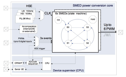
Each of the six available SMED state machines includes four states used during normal operation, along with a HOLD state. The conditions that trigger a change of state are user-configurable, and during a state transition the PWM output is updated. Once configured, the SMED runs autonomously at 96MHz. Although each SMED runs independently, they can also be combined to create more powerful state machines.
The integrated STM8 microcontroller is used not only to configure each SMED but also to monitor their activity, and communicate that to an external device over SPI or I2C. This technology constitutes an advanced programmable PWM generator signal, shaped by internal and external events, rather than a simple timer.
These advanced power devices have been designed to deliver the advantages of digitally-implemented switched-mode converters, such as higher efficiency and enhanced safety, in mid- and high-end power converters.
Mixed-Signal Solutions
Programmability is the enabling factor in modern digital power management controllers, and these devices can now be seen as exemplars of true mixed-signal design. Unlike general-purpose microcontrollers that feature mixed-signal peripherals, every aspect of these advanced digital PMCs has been designed to work systemically. This reduces or even removes the need for an intermediate stage, implemented in software to interface the digital and analogue domains, which can introduce performance ceilings. By removing that barrier, PMCs are able to reach the full potential of the underlying technology.
As such, their design represents the pinnacle of applying system-level engineering within a single chip solution. One of the most advanced examples available today is the UCD3138064ARGCT Highly Integrated Digital Controller for Isolated Power, from Texas Instruments. As well as offering more memory than its predecessor, it is the latest derivative in this family to feature dual banks of Flash memory, which allow a seamless transition from one code image to another without interrupting the power supply. This can be used for in-the-field updates, without incurring any downtime; a feature that is becoming increasingly important for networking equipment and, as such, is one of the application areas TI is targeting.
At the heart of this device is an ARM7TDMI-S microcontroller, but it is the three advanced Digital Power Peripheral blocks that really differentiate it. These comprise a high-speed digital control loop consisting of a dedicated error ADC, a PID-based 2-pole/2-zero digital compensator and DPWM outputs with 250ps pulse width resolution. It achieves this by using 16 phase-shifted clock signals, allowing it to generate waveforms with resolutions that aren’t dictated by the system clock.
The part has been designed to address a wide range of control schemes and power supply topologies, and it includes a number of additional features to support this.
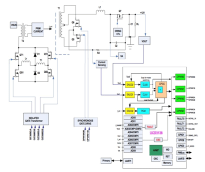
Within each DPP, the final stage is a DPWM module – a complete DPWM channel with two independent outputs. These can be used to control separate power supply output voltage rails, or synchronised with a user-defined phase shift. Combining multiple DPWMs allows various power topologies to be supported.
Conclusion
The regulations governing power efficiency in electronic devices are, quite rightly, becoming more rigorous in response to environmental and economic factors. Compliance with those regulations doesn’t have to be onerous for OEMs. There are an increasing number of advanced power management controllers being brought to market, with a corresponding level of support for power supply designers.
The number of devices coming online in the next five years could represent an unprecedented level of growth; existing power sources may struggle to supply this demand if there isn’t a sea change in the way power is handled. Fortunately, the industry hasn’t been sleeping on the job, as the example solutions presented in this article demonstrate.
Just as the IoT constitutes a massive opportunity for device developers, it is also a chance to adopt a smarter way of thinking about power consumption, and that has to be a good thing.
Mouser Electronics
Authorised Distributor


