 A new FPGA design methodology allows software engineers to build high-performance computing engines based on FPGAs, using familiar tools and techniques
Booming demand for data services such as Cloud-based storage and analytics is driving exponentially increasing computing loads that are beyond the capabilities of conventional CPUs alone. Their limited capacity for parallelisation means adding extra processors and more virtual machines cannot provide enough processing capability or prevent power consumption rising to unacceptable levels.
Data-centre equipment manufacturers have long been keen to take advantage of the massive parallelism possible with FPGAs to achieve the processing performance and I/O bandwidth needed to keep pace with demand, within a highly efficient power budget. Traditionally, however, implementing a hardware computing platform in an FPGA has been a complex challenge that has required designers to deal with some of the lowest levels of hardware implementation.
Although some recent FPGA-design methodologies incorporating High-Level Synthesis (HLS) tools and software programming languages such as OpenCL™, C, and C++ have simplified the task, they have not eliminated the need for specialist FPGA-design expertise.There is a need for a high-level workflow that allows software engineers to use an FPGAasa software-defined computing platform without the pain of hardware design. To satisfy this need, such a workflow should be able to:
- Create functional hardware from pure software code
- Incorporate existing hardware IP blocks if needed
- Infer and create all of the support hardware (interfaces, control, clocks, etc.)
- Support the use of commercial, off-the-shelf boards and custom platforms
- Eliminate hardware debug by ensuring generated hardware is correct by construction
- Support debug of functional blocks using standard software debug tools only
Consider a software algorithm comprising two basic functions: data is processed into one function and then sent to another for further processing. From a software perspective, this implementation is as simple as a call to Function1 followed by a separate call to Function2, using pointers to the location of the data to be processed.

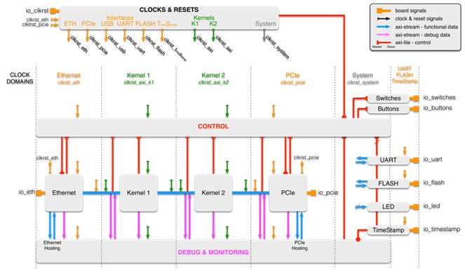
Implementing such an algorithm on an FPGA-based hardware platform without the right hardware abstraction tool flow would require the software developer to come up with a hardware design resembling that in Figure 2 (where Kernel 1 and Kernel 2 are the respective hardware implementations of Function 1 and Function 2).

The hardware design would need to include both the control plane and the data plane.The control plane is the execution engine that generates clocks and resets, manages system start up, orchestrates data plane operations, and performs all housekeeping functions. The data plane instantiates and connects the processing elements, Kernel 1 and Kernel 2, as well as the necessary I/O interfaces required to read data in and write processed data out. In the example shown in figure 2, those interfaces are Ethernet and PCI Express (PCIe).
Familiar Challenges
A software developer without specific hardware expertise could generate Kernel 1and Kernel 2,using a high-level synthesis tool such as Vivado® HLS to compile the software functions Function1() and Function2() as written in C or C++ into FPGA hardware descriptions in VHDL or Verilog. However, the non-algorithmic elements of the design, such as interfaces, control, clocks and resets could not be generated with HLS tools. Hardware designers would be needed to create these as custom hardware description language functions or IP. The job of sourcing those elements and connecting them poses yet another challenge, as some elements may not be readily available or may have different types or sizes of interfaces as well as different clocking requirements, specific start up sequences and so on.
Implementing the design presents equally tough challenges. These include mapping the design onto the resources of the selected FPGA platform, generating the appropriate constraints, and confirming that those constraints are met after logic synthesis and implementation on the FPGA hardware. Evenan experienced hardware designer can take weeks to achieve even the simplest design on a new piece of FPGA hardware.
A New Approach
PLDA Group, a developer of embedded IP, has created Quick Playto allow software developers to accomplish these tasks, and hence implement applications intended for CPUs, partially or fully, on FPGA hardware.In thissoftware-centric methodology, the designer first develops a C/C++ functional model of the hardware engine, and then verifies the functional model with standard C/C++ debug tools.Thetarget FPGA platform and I/O interfaces (PCIe, Ethernet, DDR, QDR, etc.) are then specified, and finally the hardware engine is compiled and built.
For this process to work seamlesslythe generated hardware engine must be guaranteed to function identically to the original software model. This means the model must be deterministic, so that it will yield the same results as the hardware however fast the hardware implementation runs.Unfortunately, most parallel systems suffer from nondeterministic execution. Multithreaded software execution, for example, depends on the CPU, on the OS and on nonrelated processes running on the same host. Multiple runs of the same multithreaded program can have different behaviours.
Such non-determinism in hardware would require debugging the hardware engine itself, at the electrical waveform level. This would defeat the purpose of a tool aimed at software developers, but QuickPlay’s dataflow model guarantees deterministic execution regardless of the execution engine. The model consists of concurrent functions, called kernels, communicating with streaming channels, which correlates well with how a software developer might sketch an application on a whiteboard. The contents of any kernel can be arbitrary C/C++ code, third-party IP, or even HDL code.
The QuickPlay design flow is straight forward as shown in figure 3.
A Closer Look at the Design Flow
Stage 1: Pure software design. The FPGA design is created by adding and connecting kernels in C, and specifying the communication channels using the host development software. The QuickPlayIDEprovides a C/C++ library and API to create kernels, streams, streaming ports and memory ports, and to read and write to and from streaming ports and memory ports.
Stage 2: Functional verification ensures the software model works correctly.The model is compiled on the desktop and executed with a test program that sends data to the inputs, allowing the correctness of the outputs to be verified.
Stage 3: The FPGA hardware is then generated from the software model. At this stage the target FPGA, and also the physical interfaces and protocols to map to the design input and output ports, are selected using simple drop-down menus.
Stage4: System execution is similar to functional verification, except that the FPGA design runs on the selected FPGA board, while the host application still runs in software. Real data can be streamed in and out of the FPGA board. Many more tests can be run at this stage than during functional verification.
Stage5: System debug.Debugging at the hardware level is never necessary, even if a bug is discovered after executing a function in hardware, because QuickPlay guarantees functional equivalence between the software model and the hardware implementation. Any bug in the hardware version also exists in the software version.
Stage 6: (Optional) Optimization. While the entire infrastructure built by QuickPlay is highly efficient in terms of performance and utilization, the overall quality of the design will depend on the quality of the user-created kernels. Asgeneric C code will not produce the most efficient hardware implementation, there are a few techniques and guidelines that software developers can follow to greatly improve the efficiency of the HLS generated code. Further optimization can also be done by using Vivado HLS or by recoding certain kernels in HDL.
Summary
This simple methodology has opened up FPGA-based computing to a large audience of software engineers, who can now do their modelling in software, using familiar techniques, then build the system and test in hardware. No other tool has taken this approach as far and offers a framework where software engineers can design and debug exclusively at the source level.
The efficiency of the hardware generated also makes QuickPlay a great tool for hardware engineers looking at saving weeks/months of design effort by letting QuickPlay take care of the mundane hardware design tasks, while they concentrate on their true value add: the processing kernels.
QuickPlay’s dataflow model of computation makes it ideal for a large number of FPGA applications, whether it is for pure CPU co-processing, pre or post-processing of acquired data by a CPU or simply in systems with no CPU involved (applications such as Networking, Broadcast, Vision, Medical, Wireless, HPC, and more).
For more information visit http://www.quickplay.io


