By Ron Wilson, Altera
FinFET is the latest buzzword in electronics design industry today. Everyone is talking about FinFETs—arguably the biggest change in transistors since commercialization of the MOSFET in the 1960s. And nearly everyone—except perhaps enthusiasts of fully-depleted silicon on insulator (FDSOI)—accepts that beyond the 20 nm node, FinFETs are the future of SoCs. But what does that future hold for a system developer who will use these SoCs?.
The best way to answer that question may be to find out what FinFETs will mean to circuit designers—analog and digital—and then to SoC designers. From this information we can infer what FinFETs will mean at the system level.
What’s make FinFETs Different?

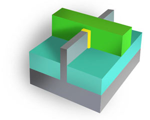
Enough has been said about the thinking behind FinFETs and about their structure (Figure 1) that we needn’t repeat those discussions here. We are more interested in how FinFETs differ from planar MOSFETs in the eyes of the circuit designer. For that question a technical panel at this year’s Design Automation Conference (DAC) provided a unique window into the thinking of analog designers.
“Analog Design with FinFETs,” rather curiously subtitled “The Gods Must Be Crazy” presented the views of four experts: foundry representatives Eric Soenen of TSMC and Richard Trihy of Globalfoundries, tool expert Navraj Nandra of Synopsys, and design manager Scott Herrin of Freescale. The discussion opened on the electrical characteristics of the new transistors.
On the positive side, Herrin pointed out that FinFETs offered the promise of high gain with low subthreshold leakage current.
Nandra added “The intrinsic gain is high, but transconductance (gm) is actually lower for FinFETs, as is frequency (ft). Matching is much better than with advanced-geometry planar devices, and the transistor characteristics are better-controlled. The result is that you can build higher-performance circuits. And there are other pleasant surprises. For example, current sources are smaller, so you can build smaller data converters.”
But there are challenges, too. Both gm and gd are lower, gate leakage is higher, and gate capacitance can be twice that of a same-sized planar device, Nandra said. And perhaps the most-publicized point, as Soenen remarket, is that FinFET gate widths are quantized: every transistor on a wafer has the same nominal gate width. So analog designers who are used to picking values of w for individual transistors can only put a number of identical FinFETs in parallel—in effect, w as a circuit parameter goes from a continuous variable to a set of small positive integers.
Layout Issues
Quantization, by replacing width-scaled transistors with multiple minimum-width transistors, will change layout practices. For example, Nanda said, Synopsys has a tool to convert gate-width ratios into the necessary number of fins. But in a presentation separate from the panel, Cadence vice president for silicon sign-off Anirudh Devgan cited more serious layout issues.
“The complexity of multipatterning will get worse as we move to more advanced geometries,” Devgan said. “And as it gets worse, it will become much harder to predict design-rule errors. Errors become context-dependent.”
Some of the rules are familiar: spacing rules to reduce coupling and shape rules for lithography, for example. Double-patterning adds coloring rules to ensure that the finest patterns can be broken into two separate masks. And there are relatively new layout-dependent effects, among which Devgan cited six—including well proximity and poly spacing—that have significant impact on transistor behavior. To show the scale of the problem, Devgan said there are already about 5,000 layout rules to check at 20 nm.
One result of this complexity for analog designers and digital cell-library developers is that it becomes nearly impossible to create DRC-clean-by-construction layouts. Designers must anticipate multiple iterations as extraction and DRC reveal layout problems. “This costs weeks,” Devgan warned. “Already 40 percent of design time goes into achieving closure.”
Modeling Challenges
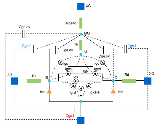
In addition to these differences in transistor behavior, FinFETs present another set of issues for the circuit designer: the simulation models are structurally different from those for planar MOSFETs, and much more complex (Figure 2). “If you look at the model, there is a ten-times increase in the number of parasitic capacitors,” Trihy warned. “It is not clear that table-driven simulators can even handle FinFETs.”
Even with this level of complexity, not all models will be accurate in all situations. So to an extent not familiar to planar-transistor users, the choice of models becomes circuit- and perhaps layout-dependent. “There are differences, and you have to know the limits of your models,” Herrin agreed.

Nandra said that Synopsys has been using SPICE in combination with TCAD process models and the common multigate model in BSIM-4 to get accurate simulations of FinFET circuits. BSIM-4 does achieve accurate modeling of behavior, even in the subthreshold region, he said. But the model is uncomfortably complex for use in a circuit simulation. “You have to prune the parasitics in a structure-dependent way,” Nandra admitted.
Trihy continued on that theme. “Where exactly does the device model stop, and circuit extraction start?” he asked. “With FinFET circuits the boundary is unclear. You can depend on design rules to limit interactions, but in the end it may be not the accuracy of your models but the accuracy of extraction that matters most.” And Devgan, in his separate talk, warned that in some cases it might require field solvers to achieve accurate extraction on the complicated, tightly-packed 3D structures that can arise in FinFET circuits.
New Approaches, New Circuits
With significant changes in transistor behavior, layout rules, and modeling techniques, it is unlikely that a circuit topology that works in a 28 nm planar process will just scale to a 14 nm FinFET process. Quantization will impose some changes. Lower voltages, limited gm, and high gate capacitance will mandate other changes, including limiting fan-outs and dealing with a compressed dynamic range. “This is not a power technology,” Soenen cautioned, “but that said, we are planning to offer 1.8 V FinFETs.” Herrin commented that the voltage limitations could mean, for example, totally different ESD circuits and a new approach to supporting higher-voltage I/Os in embedded applications.
Soenen and Nandra agreed on the impact of these changes. “You are going to see a lot of digital assist in analog circuits,” Soenen predicted. “Expect to see switched-capacitor filters and wider use of oversampling techniques.”
“We are starting to see circuits that didn’t exist before FinFETs,” Nandra added.
The Chip Level
For designers of analog circuits and digital cell libraries, FinFETs in advanced geometries will bring blessings and bothers. On the blessing side will be smaller circuits, higher operating frequencies, probably less worry about variability, and certainly lower subthreshold leakage. On the bother side, design will be more difficult and closure may require more iterations. Often, design reuse from earlier generations just won’t work. Designers will have to create new circuit approaches, topologies, and layouts. New design means more time and risk, but also the potential for improvements far in excess of the transistor-level advances in speed, density, and power.
For the chip-level designer who uses the blocks and cell libraries, the picture is quite different. Most of the added complexity of advanced-geometry FinFETs is confined within the blocks and cells. The chip designer mostly sees smaller, faster blocks with significantly lower static power. That last point, by the way, means many designs can get by with less aggressive power management than in previous recent generations.
There will still be issues. Low operating voltages will make signal- and power-integrity analyses more critical. Lower fan-outs may complicate timing closure for synthesized logic. And more difficult closure at the block level means extra care not to break anything during final integration. But these are all familiar issues that have grown with each new process generation. They are not show-stoppers.
The Bottom Line
Finally, what are the implications for system designers who will use FinFET-based SoCs? Both our analysis here and the experience in industry with Intel’s 20 nm Tri-Gate SoCs point to the same conclusion.
Each successive step in the design chain—from transistor to cell or circuit, from circuit to functional block, from blocks to chip, and from chip to system—tends to pass along the advantages of FinFETs and filter out the challenges. The chip designer gets faster, lower-leakage libraries without having to know what the cell designer went through to create them.
Similarly, the system designer will see chips with greater component density—area should continue to scale with metal or poly pitch, contact pitch, or gate length, depending on the structure—increased maximum performance, and substantially reduced leakage current. There may be some second-order effects. For example, significantly lower core voltage may put new demands on voltage regulators for low noise and excellent transient response. Some SoCs may not support legacy high-voltage I/Os.
But taken on the whole, the FinFET revolution delivers to system developers just what it promised: for density, speed, and power, a return to scaling. There is one more interesting point. By requiring circuit designers—especially analog designers—to abandon familiar circuits, FinFETs are opening the door to major, discontinuous innovation at the circuit level. Novel circuits may carry some SoCs well beyond the improvements due to renewed scaling, into new, application-opening territory.


