Cost effective services with qualities like reliability, punctuality and honesty expected from human are the victim of present day modern generation and people are running after machines to get all these services. Electronic eye is also one of such scientific and technological invention where it can replace human eye which is either damaged accidently or is not enough for services due to human mentality. Until science is not able to replace a human mind/brain which controls the other human organs to give desired output, efforts are to have scientific replicas of human organs in order to find a temporarily solution to problems. In this pursuit, electronic eye is also a replacement for human eye and is very much in use for various applications. When electronic eyes are being placed at every nook and corner to check the thieves, first useful artificial eye is also now helping a blind man walk safely around and read large letters.
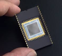
 In its most elementary form, the charge-coupled device (CCD) sensor is like the camera’s “electronic eye”—collecting light and converting it to charge, and subsequently emitting the signal that results in a digital image. The strength of the current depends upon the amount of light that falls on the electric eye. When the light stops, so does the current. This is achieved by “shifting” the signals between stages within the device one at a time. CCD displays the data for an image in such a way that each pixel (picture element) in the image is converted into an electrical charge, the intensity of which is related to a color in the color spectrum. For a system supporting 65,535 colors, there will be a separate value for each color that can be stored and recovered. A specially developed CCD can be used for ultraviolet imaging in a wire bonded package. Technically, CCDs are implemented as shift registers that move charge between capacitive bins in the device, with the shift allowing for the transfer of charge between bins. Often the device is integrated with a sensor, such as a photoelectric device to produce the charge that is being read, thus making the CCD a major technology where the conversion of images into a digital signal is required.
The required CCD array technology was invented in 1969 by Willard Boyle and George E. Smith at AT&T Bell Labs (USA) for which they shared Physics Nobel Prize 2009 along with Charles K Kao for fiber optics. The laboratory was working on the picture phone and on the development of semiconductor bubble memory. Merging these two initiatives, Boyle and Smith conceived of the design of what they termed ‘Charge Bubble Devices’. The essence of the design was the ability to transfer charge along the surface of a semiconductor. As the CCD started its life as a memory device, one could only “inject” charge into the device at an input register. However, it was immediately clear that the CCD could receive charge via the photoelectric effect and electronic images could be created. By 1969, Bell researchers were able to capture images with simple linear devices; thus the CCD was born. Several companies picked up on the invention and began development programs. Eventually, Sony managed to mass produce CCDs for their camcorders.
Basic Principle:
An image is acquired when incident light in the form of photons falls on the array of pixels. The energy associated with each photon is absorbed by the material and a reaction takes place that creates an electron-hole charge pair (for example, an electron). The number of electrons collected at each pixel is linearly dependent on light level and exposure time, nonlinearly dependent on wavelength. Once the charge has been integrated and is held in the pixel architecture, there must be a means of getting the charge to the sense amplifier, which is physically separated from the pixels. As the charge associated with one pixel move, at the same time, the charge in all the pixels associated with that row or column move as well. The packets of charge are eventually shifted to the output sense node, where electrons are converted to voltage. Conventional techniques usually use a floating-diffusion sense node followed by a charge-to-voltage amplifier, such as a source follower. Source followers are used to preserve the linear relationship between light in, electrons generated, and voltage output.
| The charge packets (electrons, blue) are collected in potential wells (yellow) created by applying positive voltage at the gate electrodes (G). Applying positive voltage to the gate electrode in the correct sequence transfers the charge packets. In a CCD for capturing images, there is a photoactive region (an epitaxial layer of silicon), and a transmission region made out of a shift register (the CCD). An image is projected |
through a lens onto the capacitor array (the photoactive region), causing each capacitor to accumulate an electric charge proportional to the light intensity at that location. A one-dimensional array, used in line-scan cameras, captures a single slice of the image, while a two-dimensional array, used in video and still cameras, captures a two-dimensional picture corresponding to the scene projected onto the focal plane of the sensor. Once the array has been exposed to the image, a control circuit causes each capacitor to transfer its contents to its neighbor (operating as a shift register). The last capacitor in the array dumps its charge into a charge amplifier, which converts the charge into a voltage. By repeating this process, the controlling circuit converts the entire contents of the array in the semiconductor to a sequence of voltages, which it samples, digitizes, and stores in memory.
The photoactive region of the CCD is, generally, an epitaxial layer of silicon. It has a doping of p+ (Boron) and is grown upon a substrate material, often p++. In buried channel devices, the type of design utilized in most modern CCDs, certain areas of the surface of the silicon are ion implanted with phosphorus, giving them an n-doped designation. This region defines the channel in which the photogenerated charge packets will travel. The gate oxide, i.e. the capacitor dielectric, is grown on top of the epitaxial layer and substrate. Later on in the process polysilicon gates are deposited by chemical vapor deposition, patterned with photolithography, and etched in such a way that the separately phased gates lie perpendicular to the channels. The channels are further defined by utilization of the LOCal Oxidation of Silicon (LOCOS) process to produce the channel stop region. Channel stops are thermally grown oxides that serve to isolate the charge packets in one column from those in another. These channel stops are produced before the polysilicon gates are, as the LOCOS process utilizes a high temperature step that would destroy the gate material. The channels stops are parallel to, and exclusive of, the channel, or “charge carrying”, regions. Channel stops often have a p+ doped region underlying them, providing a further barrier to the electrons in the charge packets (this discussion of the physics of CCD devices assumes an electron transfer device, though hole transfer, is possible)
One should note that the clocking of the gates, alternately high and low, will forward and reverse bias to the diode that is provided by the buried channel (n-doped) and the epitaxial layer (p-doped). This will cause the CCD to deplete, near the p-n junction and will collect and move the charge packets beneath the gates – and within the channels – of the device. It should be noted that CCD manufacturing and operation can be optimized for different uses. The above process describes a frame transfer CCD. While CCDs may be manufactured on a heavily doped p++ wafer it is also possible to manufacture a device inside p-wells that have been placed on an n-wafer. This second method, reportedly, reduces smear, dark current, and infrared and red response. This method of manufacture is used in the construction of interline transfer devices. Another version of CCD is called a peristaltic CCD. In a peristaltic charge-coupled device, the charge packet transfer operation is analogous to the peristaltic contraction and dilation of the digestive system. The peristaltic CCD has an additional implant that keeps the charge away from the silicon/silicon dioxide interface and generates a large lateral electric field from one gate to the next. This provides an additional driving force to aid in transfer of the charge packets.
Working of a CCD:
CCDs begin on thin wafers of silicon processed with a series of steps that define the various functions within the circuit. On each wafer lie several identical devices, or die, each capable of yielding a functional device. Selected die are then cut from the wafer and packaged in a carrier for use in a system. Like the engine of a car, the CCD sensor in a digital camera acts as the primary tool to capture an image. It works under following steps:
- Mechanical shutter opens, exposing the CCD sensor to light
- Light is converted to charge in the CCD
- The shutter closes, blocking the light
- The charge is transferred to the CCD output and converted to a signal
- The signal is digitized, and the digital data is captured in memory
- The captured image is processed and displayed on the camera LCD or computer
- CCD imaging is performed in a three-step process
- Exposure, which converts light into an electronic charge at discrete sites called pixels
- Charge transfer, which moves the packets of charge within the silicon substrate
- Charge-to-voltage conversion and output amplification
Architecture:
The CCD image sensors can be implemented in several different architectures. The most common are full-frame, frame-transfer, and interline. The distinguishing characteristic of each of these architectures is their approach to the problem of shuttering. In a full-frame device, all of the image area is active, and there is no electronic shutter. A mechanical shutter must be added to this type of sensor or the image smears as the device is clocked or read out. With a frame-transfer CCD, half of the silicon area is covered by an opaque mask (typically aluminum). The image can be quickly transferred from the image area to the opaque area or storage region with acceptable smear of a few percent. That image can then be read out slowly from the storage region while a new image is integrating or exposing in the active area. Frame-transfer devices typically do not require a mechanical shutter and were a common architecture for early solid-state broadcast cameras. The downside to the frame-transfer architecture is that it requires twice the silicon real estate of an equivalent full-frame device; hence, it costs roughly twice as much. The interline architecture extends this concept one step further and masks every other column of the image sensor for storage. In this device, only one pixel shift has to occur to transfer from image area to storage area; thus, shutter times can be less than a microsecond and smear is essentially eliminated. The advantage is not free, however, as the imaging area is now covered by opaque strips dropping the fill factor to approximately 50 percent and the effective quantum efficiency by an equivalent amount. Modern designs have addressed this deleterious characteristic by adding micro-lenses on the surface of the device to direct light away from the opaque regions and on the active area. Micro-lenses can bring the fill factor back up to 90 percent or more depending on pixel size and the overall system’s optical design.
Uses:
The charge-coupled device (CCD) was originally conceived as a new type of computer memory circuit but it soon became apparent that the CCD had many other potential applications, including signal processing and imaging—the latter because of silicon’s light sensitivity. Although CCDs are not the only technology to allow for light detection, CCDs are widely used in professional, medical, and scientific applications where high-quality image data is required. CCDs are now commonly included in digital still and video cameras. They are also used in astronomical telescopes, scanners, and bar code readers. The devices have also found use in machine vision for robots, in optical character recognition (OCR), in the processing of satellite photographs, and in the enhancement of radar images, especially in meteorology. A CCD in a digital camera improves resolution compared with older technologies. Some digital cameras produce images having more than one million pixels. The term megapixel has been coined in reference to such cameras. Another asset of the CCD is its high degree of sensitivity. A good CCD can produce an image in extremely dim light, and its resolution does not deteriorate when the illumination intensity is low, as is the case with conventional cameras. Due to the high quantum efficiencies of CCDs, linearity of their outputs (one count for one photon of light), ease of use compared to photographic plates, and a variety of other reasons, CCDs were very rapidly adopted by astronomers for nearly all UV-to-infrared applications.


