
Munich, Germany – 1 June 2021 – Infineon Technologies AG (FSE: IFX / OTCQX: IFNNY) expands its growing portfolio of single-channel gate-driver ICs. The new EiceDRIVER™ 1EDB family of single-channel gate-driver IC provides galvanic input-to-output isolation of 3 kV rms (UL 1577) that ensures rugged ground-loop separation. Their common-mode transient immunity (CMTI) exceeds 300 V/ns, making these devices the perfect choice for hard switching applications enabling numerous topologies.
The new 1EDB family includes four parts (1EDB6275F, 1EDB7275F, 1EDB8275F and 1EDB9275F) and is optimized for both high/low-side applications. They can solve PCB-layout problems, common in high-power applications such as server and telecom switched-mode power supplies (SMPS) as well as uninterruptable power supply (UPS) systems. Due to their increased power-density need, EV-charging designs often require fast-switching power MOSFETs. Photovoltaic inverters take advantage of silicon carbide MOSFETs as they enable both lower switching losses and a significant step forward in power density. The new 1EDB family addresses all these applications, ensuring high system efficiency and robust and safe system operation.
All products come with separate and very low ohmic (0.95 Ω) source and (0.48 Ω) sink outputs for ease of design, offering typical drive strengths of 5.4 A peak source and 9.8 A peak sink. This feature plays a vital role in reducing the switching losses of power MOSFETs. The input-to-output propagation delay accuracy is +/- 4 ns helping to cut switching losses, which is essential in fast-switching applications. The typical output stage clamping speed is as short as 20 ns and supports functionally safe system operation, especially during start-up.
Designers can choose between four different output under-voltage lockout (UVLO) options:
- 0 V for logic-level MOSFETs (1EDB7275F)
- 0 V for normal-level MOSFETs (1EDB8275F)
- 12 V for CoolSiC™ MOSFETs 650 V (15 V driving scheme, 1EDB6275F)
- 14 V for CoolSiC™ MOSFETs 650 V (≥18 V driving scheme, 1EDB9275F)
Availability
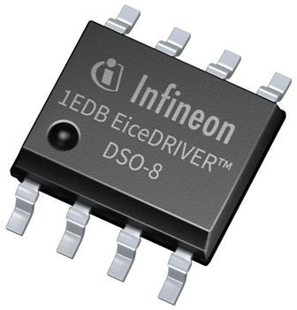
EiceDRIVERs 1EDB7275F and 1EDB8275F are available in 150 mil 8-pin DSO packages and can be ordered now. Variants 1EDB6275F and 1EDB9275F will follow shortly. Further information can be found at www.infineon.com/1EDB


