FinFET Design and EDA support
Simply put, FinFET is a three-dimensional field-effect transistor (FET) where the gate is wrapped around an elevated channel, creating a “fin”. Compared to traditional planar MOS transistors, FinFET architecture offers reduced leakage power and increased drive current, resulting in lower power, higher performance SoCs for mobile, networking, computing, and other applications.
Leading manufacturers such as GlobalFoundries, Intel, Samsung and TSMC and their EDA partners are spending a lot of effort to support the new technology. To make the transition to FinFET based designs as smooth as possible for the design community, EDA and IP vendors are working closely with foundries to ensure that the tools can support the associated complexities. For example, ANSYS power integrity and electromigration tools were recently certified by TSMC for 16nm FinFET technology.
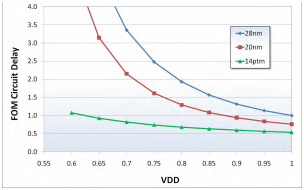
The use of FinFETs enable design teams to operate their chips at significantly lower supply voltages. This has an immediate benefit in reducing their dynamic power consumption without impacting their standby currents (Figure 1).

However, lower supply voltage also means smaller noise margin. For example, 200mV noise at the sub-700mV supply levels can be fatal for the chip’s performance and functionality. In addition, on-chip decoupling capacitors are becoming increasingly ineffective in ensuring local charge availability for fast charging devices.
Addressing reliability with ANSYS RedHawk 2014
ANSYS RedHawk 2014 addresses such emerging power-noise-reliability needs arising from the use of FinFET structures. The number-one priority for any simulation solution is sign-off accuracy. Without it, designers cannot rely on the tool to provide correct results. With higher voltage drop noise and reduced noise margins, sign-off quality voltage drop analysis demands the inclusion of accurate and representative IP models and package/PCB parasitics. So the latest release introduces RedHawk-CPA, the industry’s first chip-package co-analysis solution. It enables native chip-package co-analysis by bringing in both chip and package layouts into the same simulation platform, providing immediate feedback regarding the impact of on-chip current distribution — over time and over chip area — on the package design, as well as the impact of the package parasitics on the chip’s performance.
The newest RedHawk release offers distributed machine processing (DMP), which enables the analysis of 100 M+ instances or 2 B+ node designs by significantly reducing the total turn-around time while maintaining its silicon-validated sign-off accuracy. It effectively distributes a large design database across several machines and simulates each partition in the context of the entire chip, including package and PCB. This unique in-context analysis methodology enables RedHawk 2014 to reduce memory usage and run-time by two to three times. Unlike hierarchical methods that cannot model time-varying current flow across the block boundaries, RedHawk’s DMP capability delivers sign-off accurate full-chip voltage drop, EM and ESD analyses.
FinFET architecture does more than reduce the noise margin: It increases local self-heating, which worsens reliability issues such as electromigration (EM) and electrostatic discharge (ESD). As seen from foundry data, the EM limits for vias are generally 70% of what they were for prior technologies while the current levels are 25 to 30% higher. RedHawk 2014 accurately analyzes EM violations for power/ground and signal line, while minimizing false positives. Its proprietary current-flow aware extraction techniques help to achieve sign-off quality results for every wire and via in a design.
Adding traditional ESD protection devices is not possible in FinFET technology, so there is a shift to using larger and less effective diodes. To prevent ESD induced failures, the designers need to carefully design, select the placement and analyze the connectivity of these devices. Traditional approaches of using ‘design guidelines’ or ‘plot checks’ are too limiting and error prone. Layout based simulation techniques that consider the parasitics of the on-chip interconnects, incorporate their connectivity to the ESD protection devices and predict the flow of current in these wires during an ESD event are required to identify, isolate and fix any possible failure scenarios.
ANSYS PathFinder, which is part of the RedHawk platform, supports IP to SoC-level ESD integrity analysis by providing both connectivity and interconnect failure checks for all current flow pathways (wires and vias) from an ESD event (HBM or CDM).
The ANSYS power noise and reliability ecosystem extends beyond the RedHawk simulation platform to include production-proven system-level simulation solutions, empowering designers with system-aware chip simulation and chip-package-aware system simulation methodologies to ensure that the chip and the system are designed to work together at the lowest cost.


