Automatically, we put equal impedances on both inputs of an op amp, as we were taught many years ago. This article explores why this rule of thumb came about and whether or not we should follow this practice.
What You Were Told
If you grew up with the 741 op amp,1 it was drilled into your head to balance resistances seen by the op amp inputs. Over time, with different circuit techniques and different IC processes, this may not be the right thing to do. In fact, it can lead to more dc error, more noise, and more instability. Why did we start doing this and what changed so that it may not be the right thing to do today?
In the 1960s and 1970s, first generation op amps were manufactured on a plain vanilla bipolar process. To get reasonable speeds, the differential pair tail current was generally in the 10 μA to 20 μA range.
Therefore, with betas of 40 to 70, the input bias current was about one
microamp. However, the transistor matching wasn’t that close, so the input bias currents were not equal, resulting in a difference in the input bias currents (called input offset current) by 10% to 20% of the input bias current.
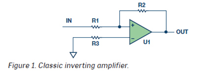
By adding a resistance (R3 in Figure 1) in the noninverting input to ground, equal to the parallel combination of the input resistor and the feedback resistor, the impedances are made equal. Doing some algebraic manipulation, it can be shown that the error is reduced to Ioffset × Rfeedback.
Because the Ioffset was 10% to 20% of Ibias, this would help in reducing the output offset error.
 DC Error
To reduce the input bias current on bipolar op amps, input bias current cancellation was integrated into many op amp designs. An example of this can be found in the OP07. With the addition of input bias current cancellation,2 the bias current is greatly reduced, but the input offset current can be 50% to 100% of the remaining bias current, so adding the resistor has very little effect. In some cases, adding the resistor could result in the output error actually increasing.
Noise
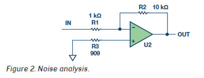
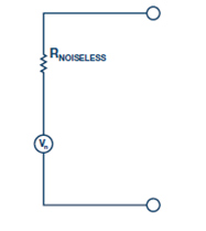
The thermal noise of a resistor is given by √4kTRB, so a 1 kΩ resistor will be 4 nV/√Hz. Adding a resistor will add noise. In Figure 2, surprisingly, even though the 909 Ω compensation resistor is the lowest value because of noise gain from that node to the output, it contributes the most noise at the Figure 2 output. Output noise due to R1 is 40 nV/√Hz, for R2, 12.6 nV/√Hz, and for R3, 42 nV/√Hz. So don’t use a resistor. On the other hand, if the op amp is powered from split supplies and one supply comes up before the other one, there may be latch-up problems with the ESD network, in which case it may be desirable to add some resistance to protect the part. But if used, a bypass cap should be placed across the resistor to reduce the noise contribution of the resistor.
 Stability
All op amps have some input capacitance, both differential and common mode. If the op amp is connected as a follower and the impedances are balanced by putting a resistor in the feedback path, the system may become prone to oscillation. The reason is that with a large feedback resistor, the input capacitance of the op amp, and the stray capacitance on the pc board, an RC low-pass filter (LPF) is formed. This filter causes phase shift and will reduce the phase margin of the closed-loop system.
If it reduces it too much, the op amp will oscillate. A customer was using an AD8628 CMOS op amp in a 1 Hz, Sallen-Key low-pass filter circuit.
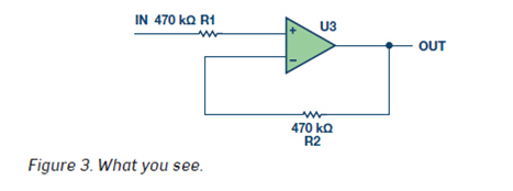
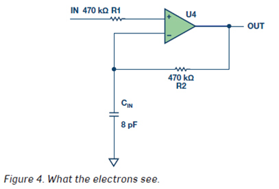
Because of the low corner frequency, the resistors and capacitors were rather large (see Figure 3). The input resistor was 470 kΩ, so the customer put a 470 kΩ in the feedback. This resistor, in combination with the eight
picofarads of input capacitance (see Figure 4), gave the customer a pole at
42 kHz. The AD8628 has a gain bandwidth product of 2 MHz, so it still had plenty of gain at 42 kHz and it oscillated rail-to-rail. Changing the 470 kΩ resistor to a 0 Ω jumper solved the problem. So avoid large resistors in the feedback where large depends on the gain bandwidth of the op amp. For high frequency op amps, such as the ADA4817-1 with a gain bandwidth over 400 MHz, a 1 kΩ feedback would be large. Always read the data sheet for recommendations.

 Summary
Over the years, rules of thumb are developed that serve a purpose.
On a design review, it’s always good practice to look carefully at these rules and see if they are still applicable. With respect to adding a balancing resistor, if the op amp is CMOS, JFET, or bipolar with input bias current cancellation, you probably don’t need one.
After reading through this article, you might be surprised that the quiz is about noise.
Here are three questions for you:
Q: Which noise is generated in a resistor?
- Popcorn noise
- Red noise
- Pink noise
- 1/f noise
- White noise
- Johnson noise
- Nyquist noise
- White noise
Q: What is the rms noise generated by a 10 kΩ resistor at room temperature (20°C) over an equivalent noise bandwidth of 20 kHz?
 Q: Having a 24-bit audio ADC with an input span of 2.5 V—how many flickering bits would we get with this VNOISE?
References
1 Ken Shirriff. “Understanding Silicon Circuits: Inside the Ubiquitous
741 Op Amp.” 2015.
2 “MT-038 Tutorial Op Amp Input Bias.” Analog Devices Inc., 2009
About Author

Harry Holt is a senior applications engineer at Analog Devices, Inc. for four years in Central Applications after six years in the precision amplifier group This follows 28 years in both field and factory applications at National Semiconductor for a variety of products, including data converters, op amps, references, audio codecs, and FPGAs. He has a BSEE degree from San Jose State University and is a life member of Tau Beta Pi and a Life Senior Member of the IEEE.


