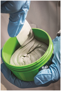
Indium Corporation is the leading innovator in solder pastes for electronics assembly. Pb-Free solder pastes can be made using a variety of Pb-Free alloys. In addition, a number of tin-lead alloys are available for Indium’s tin-lead solder pastes.
Liyakathali (Liya) Koorithodi, Assistant Technical Manager for Indium Corporation added more information about Indium solder paste technology and its features.
 Please overview your solder paste products and history of your innovations for this product?
When Indium Corporation was founded in 1934, we focused on developing basic fabrications, such as wire and ribbon, made exclusively from indium or indium alloys. Today, our company’s expanded product line serves the electronics, semiconductor, thin-film, thermal management, and solar markets by manufacturing all of the original fabrications, as well as solders, fluxes, and solder pastes, solder preforms, and thermal interface materials, made from hundreds of alloys. We also produce a line of inorganic compounds, such as indium-tin oxide which is used to manufacture LCDs.
Indium Corporation has always been known for solving challenges that others have not been able to solve. This success comes from our curiosity as scientists and engineers, but is also a testament to our commitment to seeing things through to a conclusion so that we can help our customers prosper.
Can you discuss the recent developments in solder paste technology?
With environmental and legislative actions pushing the industry toward lead-free and halogen-free solder pastes, reliability is increasingly critical. Manufacturers and assemblers are looking for solutions that enable them to become lead-free and halogen-free without seeing increased voiding and, therefore, increased product failures.
What is Indium’s market position in offering solder paste products?
Indium Corporation is the industry leader for void-reducing results for two reasons: (1) our products and (2) our experienced engineers.
Voiding is a complex problem with complex solutions. It isn’t always just a matter of switching solder pastes to solve the problem. There are many variables to consider and optimize. Voiding can be affected by oxidized components; selection or quality of the pad finish; stencil thickness; aperture design; reflow profile; and other process parameters
Indium Corporation and its technology experts are the source for process optimization. From world-renowned figures, such as Dr. Ning-Cheng Lee, to the company’s team of tech support professionals, there is no better proven source of knowledge or willingness than Indium Corporation to work through the issue with the customer to identify the solution.
According to you, what is the outlook and demand of solder paste products?
We foresee a period of protracted growth and development spanning the next several years. Demands for reduced assembly costs and increased product densification remain constants. Consequences of these challenges include reduced feature size (continued miniaturization), increased heat generation, more double-sided designs, and increased use of die and package stacking. Customers will need to identify the ideal solder paste formulation to ensure minimal voiding, as well as opportunities to further optimize their processes.
Tell us about Indium8.9HF Solder Paste and its features?
Indium Corporation’s Indium8.9HF is a halogen-free, no-clean solder paste that is specifically formulated to Avoid the Void™, while delivering high print transfer efficiency with low variability.
In addition to outstanding print transfer and response-to-pause, this no-clean solder paste provides the lowest QFN voiding from a halogen-free solder paste in the industry, while remaining stable at room temperature for up to 30 days. Indium8.9HF is also stable under refrigeration for one year.
Are there any limitations or challenges?
Indium8.9HF is perfectly suited for a variety of applications, especially automotive, due to its unique oxidation barrier technology. This solder paste delivers robust reflow capability and a wide process window, accommodating various board sizes and throughput requirements, minimizing potential defects.
.


