 As space-grade digital system designs increase in power consumption and complexity, while shifting to lower and tighter tolerance supply voltages, radiation-hardened (rad-hard) DC-to-DC converters such as Point-of-Load (POL) buck regulators, have become essential for maintaining highly-reliable and highly-efficient operation in these harsh environments. This article will discuss the design of power-management systems for space and defense applications requiring radiation tolerance, small size, high efficiency, and design versatility.
Market requirements for smaller size, lower weight, and reduced cost in space and defense applications are driving demands for improved power-management solutions. Additionally, the effects of radiation on electronic components in the space environment remain a key concern for spacecraft designers. Due to the prerequisites for long-term survivability and reduced program costs in space and defense applications, highly-reliable, rad-hard components are required.
FPGAs are commonly used in the space and defense markets. As a result, power-management designers are challenged to meet the increase in multi-core operation and faster processing speeds of these loads. At the same time, IC technology is shifting to lower and tighter-tolerance supply voltage requirements, while demanding more power capability at smaller voltages from regulators.
Today, there is a high demand for power-management devices that provide high load currents at low output voltages while maintaining high efficiency. POL buck regulators with integrated switches enable a smaller form factor, improved reliability, and flexibility that allow space designers and system architects to meet project goals.
Radiation Requirements
The primary radiation concerns in the natural space environment are Total Ionizing Dose (TID), Enhanced Low Dose Rate Sensitivity (ELDRS), and Single Event Effects (SEE). TID degradation or gain drifts of component parameters cause changes to circuit supply and leakage currents, threshold voltages, and propagation times. ELDRS can degrade certain types of bipolar devices more severely at very low dose rates than at higher dose rates. Additionally, SEEs occur when a high-energy particle passes through the active region of a semiconductor, triggering non-destructive effects such as upset, multiple-bit upset, or analog transients; or destructive effects such as latch-up, gate rupture, and burnout.
TID
Total dose testing is performed in accordance to MIL-STD-883, METHOD 1019. Program missions will determine the level of TID tolerance required. For example, low-earth orbit, low-lifetime missions may require 30 – 50 krad(Si), while deep space, longer lifetime missions may require 100 krad(Si) or more. Pre and post-radiation drifts for key parameters are critical data points for device qualification.
ELDRS
DC-to-DC converters that utilize bipolar technology with oxide isolation structures are subject to low-dose-rate degradation. So far, this effect has not been an issue with DC-to-DC converters based upon CMOS technology. Moreover, Silicon-on-Sapphire (SOS) technology, with its highly-insulating substrate properties, does not use bipolar minority carrier elements, and does not exhibit enhanced low-dose-rate sensitivity. Peregrine Semiconductor’s PE9915X POL buck regulators were created on the Company’s patented UltraCMOS® technology, a Silicon-on-Sapphire (SOS) process technology that enables higher integration and performance, natural radiation hardness, and lower power consumption.
SEE
Non-destructive or “soft-error effects” momentarily or permanently change the state of a device or cell/node while affecting its functionality. These types of errors are defined as Single Event Upset (SEU), Single Event Functional Interrupt (SEFI), and Single Event Transient (SET) errors.
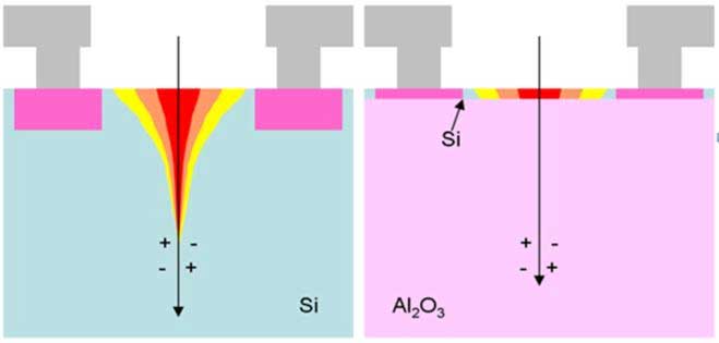
As a high-energy particle enters the silicon at a high velocity, the amount of force exerted on the electrons is not enough to cause displacement. As the particle slows down due to the depth of the silicon, more electrons become displaced, resulting in a longer recovery time, as illustrated by the field-funneling effect in Figure 1. The ultra-thin epitaxial layer in SOS technology produces the lowest-possible SEU charge collection of any production silicon technology and simplifies the circuit design needed to achieve SEU, SET, and SEFI immunity.
Destructive or “hard-error effects” interrupt device function and can permanently damage the device without external interaction. These types of errors are defined as Single Event Latch-up (SEL), Single Event Gate Rupture (SEGR), and Single Event Burnout (SEB) events.
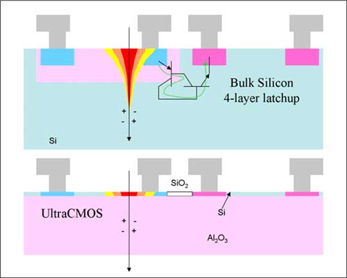
An important advantage of SOS technology is that it is naturally rad hard. SEL is the radiation-induced latch-up of a CMOS logic gate. This can happen when a high-energy particle strikes the parasitic thyristor that is inherent to bulk silicon designs and causes a short circuit from power to ground within the device. This is often catastrophic and results in permanent damage, requiring, at a minimum, a power down to recover. However, products created using SOS technology, such as Peregrine Semiconductor’s products, do not contain the bulk parasitics found in regular CMOS devices, making latch-up impossible.
Design Versatility
Several important design trade-offs are available to component and system engineers, while allowing optimization of system performance. However, the need for radiation hardness limits the availability of solutions for the space and defense markets. Integrated POL buck regulators that are hardened by design and process are capable of supplying low output voltages at high efficiencies while meeting the demands of reduced size, weight and cost. In addition to radiation tolerance, the following features should be considered when selecting a POL buck regulator for space and defense power-management applications.
Adjustable Output Voltage
The output voltage can be set using external feedback resistors. Having this flexibility allows the designer to use the same components and footprint to supply different voltages.
Selectable Switching Frequency
Switching frequency determines critical system parameters including component size, efficiency, loop bandwidth, and circuit board area. A higher switching frequency allows the use of smaller inductances and output capacitances, in order to obtain a lower ripple voltage, wider loop bandwidth, and faster transient response. A lower switching frequency may be preferred for higher efficiency, as switching losses increase as the switching frequency is raised. The switching frequency may also be selected to control the amount of switching noise generated by the POL buck regulator, in order to prevent electromagnetic interference and spurious interference with signal-processing circuits.
Frequency Synchronization
The noise generated by switching power supplies can disturb sensitive circuitry when the switching frequency is not synchronized to the system’s clock frequency. Synchronization enables two or more regulators to be locked together to one frequency, to improve system performance by eliminating beat frequencies generated by the interaction of multiple POL buck regulators.
Adjustable Current Threshold
Over current protection will protect the regulator if the output should become shorted at the load side of the inductor. This can be achieved by limiting the maximum voltage applied to an internal or external resistor. This flexibility allows characterization and testing to a high current on the bench while still limiting the current to lower level in the system application.
Adjustable Loop Compensation
Externally adjustable loop compensation allows the designer to meet transient response applications while still maintaining stability requirements. Compensation loops are typically designed with a relatively high phase margin and a slightly over-damped loop response, in order to avoid overshoot.
Adjustable Soft Start
Soft start provides power control to the load by allowing the output voltage to slowly ramp to its steady-state operating value. This feature has the advantage of limiting the output voltage rise time to prevent overshoot. The output voltage rise time is usually controlled with an external capacitor.
Power-Supply Sequencing
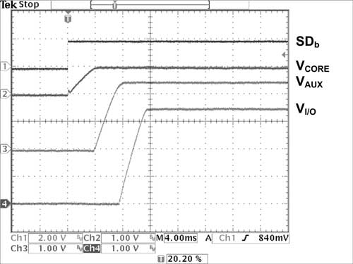
Some FPGAs and other digital loads require sequencing and/or tracking between I/O and core voltages. During start up, it may be necessary for one supply to ramp up before the other. If sequencing is ignored, the supply can “latch up” and the FPGA may be damaged or malfunction resulting in long-term reliability issues. When multiple POL buck regulators are used in distributed power architectures, simple power sequencing can be implemented using independent power-good, enable/shutdown and soft-start features. A sequential start up requires each power rail to start and reach its output voltage level in chronological order. This can be achieved by connecting the power good pin of one POL buck regulator to the enable pin of the following buck regulator. The sequential start-up waveform response in Figure 3a shows how the core voltage is powered up first, followed by the auxiliary voltage, followed by the I/O voltage.
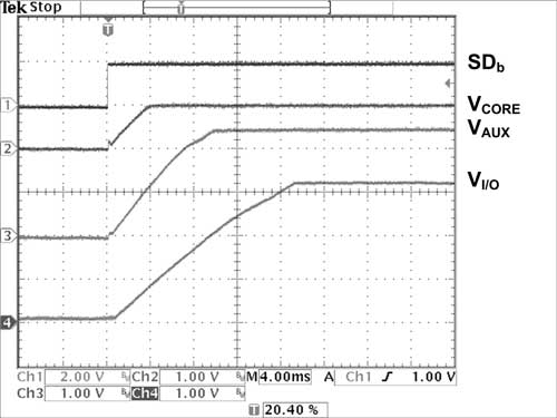
The soft-start feature can also be combined in a distributed system using power sequencing, to control the rise time of the output waveforms using a simultaneous start up scheme. This approach uses a common enable control to simultaneously activate each regulator, and an external soft start capacitor to position each slew rate. The resulting start up output waveform response is shown in Figure 3b.
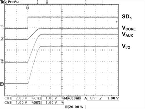
If all output voltages are required in order to reach the final regulated voltage at the same time, a ratio-metric approach may be used. This technique uses the same configuration as the simultaneous start-up approach, with the exception that all soft-start capacitors have the same value. The resulting output waveform response is shown in Figure 3c.
Current Sharing
When higher output currents are required, two or more POL buck regulators rated at the same maximum output current and operating at the same frequency may be connected in a parallel configuration, to enable a technique known as current sharing. The resulting load-current capability is the sum of the total currents of each regulator.
Proper current sharing requires that each converter deliver an equal amount of current to the load. Since the output impedance of switching regulators is very low, small differences in the output voltages between the parallel converters will result in an imbalance of current between them. If the design does not allow for currents to be equal, some converters may conduct more than others, resulting in unequal sharing.
Most POL buck regulators incorporate a robust, traditional peak-current-mode control architecture for power-management systems that must operate under extreme conditions. Current-mode control is the ideal architecture for current sharing because it maintains direct control of the switch current through a common control voltage.
Adjustable Slope Compensation
The peak-current-mode control architecture offers excellent line regulation, simple compensation design, improved transient response, and inherent cycle-by-cycle current limiting. However, all peak-current-mode control switching regulators require slope compensation to ensure stability across all operating conditions due to irregularities in the current waveform for duty cycles over 50%. Maintaining a constant peak-inductor current does not ensure a constant average-output current (peak to average current ratio), because voltage (duty cycle) fluctuations change the average value, but not the peak value. This can lead to sub-harmonic instability for wide duty cycles.
The results of slope compensation are that the average current is no longer a function of duty cycle, and that line voltage changes are perfectly rejected without requiring action by the voltage loop. Adjustable slope compensation allows the designer to optimize stability and closed loop bandwidth across the output voltage and switching-frequency ranges.
Redundancy and Hot-Swap Capabilities
Redundancy is a form of resilience designed to maintain system operation in the event of a component failure. This is often referred to as N+1 redundancy, where a POL buck regulator (N) has at least one independent backup module (+1). Fault-tolerant power-management systems may consist of two or more POL buck regulators arranged in parallel, to support redundant operation and increase system reliability.
Hot-spare or “hot-swap” refers to a power-management system in which a faulty module can be swapped with a backup module while continuing to supply uninterrupted current to the load.
Small Size
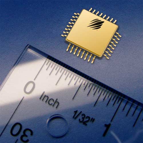
Integrated POL buck regulators, such as those in Peregrine Semiconductor’s PE9915X family, often use the same footprint, and offer drop-in, replaceable solutions. This simplifies designs by making it easier to optimize efficiency and current-limiting requirements without requiring multiple test boards.
FPGA Power Management
One of the most critical factors in an FPGA system design is power-management. High-performance signal processing devices require multiple power supplies that generate different voltages. Usually, a minimum of two voltages are needed to power FPGAs—one for the core and one for the I/O supply. Many FPGAs also require a third low-noise, low-ripple voltage to provide power to the auxiliary circuits. If the FPGA voltage requires a specific ramp rate, this can be implemented using a soft-start feature. Also, the rising voltage at start-up usually needs to be monotonic (not droop). If the supply output capacitances are small, this can cause the voltage at start-up to droop. Adequately sized capacitors store enough charge to supply the start-up load transient of the FPGA.
The FPGA can have current demands of up to tens of amps, depending upon the clock frequency and the number of gates being used. High-speed I/O resources often specify very low supply ripple and transients. Other concerns associated with some FPGAs are monotonic start-up of its supply voltages, line/load transient behavior, and power sequencing (turn-on and turn-off specifications) of the different rails.
Distributed Power Architecture
The Distributed Power Architecture (DPA) is often the power system of choice to ensure optimal system performance. The traditional single centralized isolated DC-to-DC converter or brick, which supplies the entire electrical system, exhibits large distribution power losses and low efficiency. Large bulky cables and connectors are used to overcome demands of high bus currents. The resulting system is susceptible to poor regulation and crosstalk.
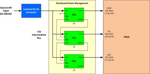
A distributed power architecture that uses the intermediate bus to supply several POL buck regulators can deliver their loads locally. This system reduces distribution losses through smaller cables and connectors, which reduce size, weight and cost. By placing the POL buck regulators close to the load, steady state and dynamic (transient) load regulation is improved and crosstalk is reduced.
Figure 5 shows how this system can be implemented. In this system, a single POL buck regulator is used to supply up to 10A to a demanding FPGA core. If more power is required, a current-sharing technique may be used. Lower-current POLs are used for the less demanding auxiliary and I/O supplies where load transient and output voltage ripple are still important. An inverted clock (SYNC) signal provides frequency synchronization to the subsequent converters. Driving additional converters 180 degrees out-of-phase can reduce the amplitude of input currents, the physical size and the electrical requirements of the input capacitance.
Efficiency
As shown in Figure 6, the load requirements of a FPGA are based upon the static and dynamic operating states. The static, or “quiescent,” state includes standby and leakage currents, while the dynamic-state current demands depend upon the clock frequency and the number of logic cells being used. As process technologies become smaller and faster, transistor leakage currents are increasing, due to the decreasing channel lengths. As a result, the static state demands high efficiency from the POL buck regulators.
Transient Response
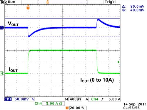
The FPGA’s core voltage can produce large current transients when the processor loading suddenly changes from a static to a dynamic state. Under these, conditions the output voltage will decrease (droop) as the load current increases, and vice versa. This is illustrated in Figure 7. The power supply must be capable of delivering a large-step load current while maintaining output voltage regulation in order to avoid FPGA lockup. The measure of how fast the regulator returns to steady-state conditions after a load change is known as the load transient response. The ability of the regulator to respond to a load transient is a function of the operating bandwidth in conjunction with the output capacitance. Sufficient bulk capacitance will help to absorb or source sudden changes in load current.
Rad hard POL buck regulators with integrated switches, such as those from Peregrine Semiconductor, offer significant benefits to modern military and spacecraft power-management applications. Peregrine’s patented UltraCMOS technology enables the integration of analog, digital and high performance on a single, monolithic rad hard die. The resulting devices provide valuable advantages, such as high reliability, and decreased size, weight, and cost. Additionally, key performance factors including frequency synchronization, power sequencing and current-sharing capabilities provide design flexibility for space, defense, and commercial/industrial applications as digital system power-management requirements become more demanding.


