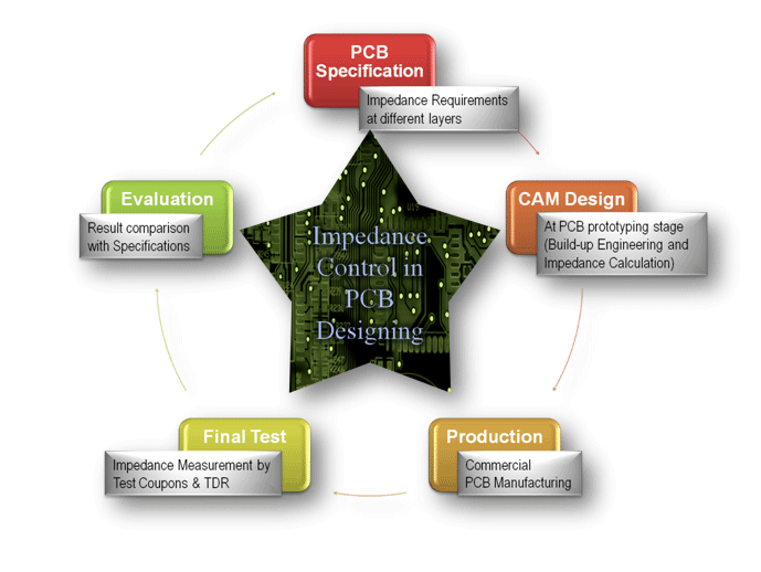
Controlled impedance PCBs are becoming more common now, especially in high-speed applications. Designing these boards can be particularly challenging for critical applications involving high speed performance. Our further article will highlight the impedance considerations in PCB design and other related aspects. Here we go …
 Controlled impedance—it’s all about transmission lines. One of the most common examples of controlled impedance is the cable that connects the antenna to our television, that’s a coaxial cable consisting of a round, inner conductor, separated from the outer cylindrical conductor commonly called the shield by an insulator. The dimensions of the conductors and insulator, and the electrical characteristics of the insulator are carefully controlled in order to determine the shape, strength and interaction of their electrical fields which will determine the electrical impedance of the cable. For perfect transfer of energy, the impedance of the driver must match the transmission line. A good transmission line is one that has constant impedance along the entire length of the line, so that there are no mismatches resulting in reflections. But unfortunately, drivers do not have the exact impedance to match the line (typically 10–35 ohms) so terminations are used to balance the impedance, match the line and minimize reflections. Reflections occur whenever the impedance of the transmission line changes along its length. This can be caused by unmatched drivers/loads, layer transitions, different dielectric materials, stubs, vias, connectors and IC packages. By understanding the causes of these reflections and eliminating the source of the mismatch, a design can be engineered with reliable performance. Impedance matching slows down the rise and fall times, reduces the ringing (over/undershoot) of clock drivers and enhances the signal quality of a high-speed design. Similarly there are many different trace configurations that are used in printed circuit boards to achieve controlled impedance.
The same considerations of wires & lines apply to signal transfer through traces on a PCB. When board traces carry signals containing high frequencies, care must be taken to design traces that match the impedance of the driver and receiver devices. The longer the trace, or the greater the frequencies involved, then the greater the need to control the trace impedance. The PCB manufacturer controls the impedance by varying the dimensions and spacing of the particular trace or laminate. Any impedance mismatch can be extremely difficult to analyze once a PCB is loaded with components. Components have a range of tolerances, so that one batch of components may tolerate an impedance mismatch, while another batch might not. Moreover, a component’s characteristics may change with temperature, so that the problems may come and go. Thus, if changing a component appears to cure a problem, the components may become the suspects instead of the trace. Component selection becomes the solution, and build costs are driven up, while all the time the real fault – trace impedance mismatch – goes undetected. For these reasons, a PCB designer will specify trace impedance and tolerance, and should work with the PCB manufacturer to ensure that the PCB meets the specifications.
| Parameters of impedance in a circuit board:
¨ Dielectric constant ξ r ¨ Signal traces geometry ¨ The copper thickness ¨ Distance from signal layer for potential location Methods of Impedance control are: ¨ Single Ended ¨ Differential impedance ¨ Odd Mode impedance ¨ Even Mode impedance ¨ Koplanar/Differential |
Printed circuit boards with impedance Control
For standard circuit boards, a PCB manufacturer is given a set of patterns – copper patterns, hole patterns, ink patterns, which are combined into a single circuit board with all the pattern sizes and positions within certain tolerances. Failure to meet a certain size or position with the specified tolerance can be cause for the circuit board to be rejected. If a trace has been defined as an impedance control trace, it is not the trace size which is strictly defined, but rather the impedance. While a nominal trace size will be provided in the Gerber layer, it is understood the circuit board manufacturer can vary trace width, height, and dielectric thickness as long as the final impedance is within tolerance. Generally 3 levels of service are available for an impedance control printed circuit board.
- No impedance control. The impedance tolerance is loose enough that simply making a design with no extra precautions will result in the correct impedance as long as the design is made correctly within the standard specifications. This is the fastest and least expensive option since it places no extra burden on the circuit board manufacturer.
- Impedance watching. The designer indicates the impedance control trace. The PCB provider adjusts the (W) width of the trace and (H) height of the dielectric and gets approval on the proposed specifications before starting manufacturing. A TDR (Time Domain Reflectometry) test can be performed to confirm the impedance for an additional cost.
- Impedance control. Usually reserved for high-end designs containing either an odd design that doesn’t fit the usual microstrip configuration or a tight tolerance. With manufacturing capability a limit approaching the dimension requirements, confidence is not high the target impedance will be achieved on the first pass. The circuit board manufacturer first makes the board, getting as close to the target impedance as possible. Next a TDR test is done to determine if the impedance is within specification and adjustments are made as necessary. In the example below, the prepreg (composite fibers “pre-impregnated” with an epoxy) can be added or removed in 1 mil increments to affect H, and changes can also be made to W. Multiple iterations may be needed depending on the design.
In the case of a microstrip, the impedance depends on 4 parameters:
- Height of the dielectric. It can be changed in steps.
- Dielectric of the material. It is fixed once the material is chosen. Having a good idea of the Er is necessary since +/- 0.1 results in +/- 0.5 Ohms.
- Trace thickness. An outer trace is plated, providing a 20% uncertainty in exterior traces. This results in a small uncertainty of +/-0.2 ohms.
- Trace width. Typical trace width uncertainty is +/-2 mil which results in an uncertainty of +/- 2 ohms.
The function of a wire or trace is to transfer signal power from one device to another. Theory shows that maximum signal power is transferred when impedances are matched.
Key Points when working with Impedance parameters
- A good transmission line is one that has constant impedance along the entire length of the line.
- The impedance of the driver must match the transmission line to avoid reflections.
- Drivers do not have the exact impedance to match the line (typically 10–35 ohms).
- Impedance matching slows down the rise and fall times, reduces the ringing (over/under shoot) of clock drivers and enhances the signal quality of a high-speed design.
- Impedance plots are simulated by multiple passes of the field solver to create heads-up plots of how to adjust the particular variables to get the desired impedance.
- If you select too low of an impedance, the di/dt will increase, drawing excessive current form the supply and no doubt, creating further power integrity issues.
- Controlling impedance is a trade-off between trace width, trace (copper) thickness, dielectric thickness, dielectric constant and trace clearance.
- The dielectric constant and loss of all materials varies with frequency.
- Multiple differential pair technologies should be accommodated on the same substrate.
- The coupling point is where increasing the trace separation or the dielectric thickness has little or no further effect on differential impedance.
 Lossless Calculation
Unmatched impedance issues will be very hard to evaluate once the board is loaded with components. Components can have a range of tolerances; one batch may tolerate an impedance mismatch, while another might not. A component’s characteristics may change with temperature, and problems may come and go with the variation in the operating temperature of the assembly. In this case replacing a component might appear to fix a problem causing the components to become the suspected cause instead of the trace. Additional costs for components and assembly might result when the real problem is a trace impedance mismatch. It becomes imperative that the PCB designer specify trace impedance and tolerance, and the board manufacturer must meet those specifications. As the operating speed of electronic circuits has increased, so has the need for printed boards to have controlled impedances and therefor the majority of board manufacturers are producing them. Impedance depends on many parameters including but not limited to trace width, trace thickness, and laminate thickness. Determination of the acceptability of the boards is done through testing procedures. However the testing is not usually performed on the actual board but on one or more test coupons manufactured at the same time and on the same panel. Coupons are used because controlled impedance traces are not always easily accessible for testing nor do they meet the requirements for length and have no branching trace work or pads to allow for the testing.
Impedance measurement of a design
Impedance measurements are usually made with a Time Domain Reflectometer or TDR. The TDR applies a fast voltage step to the coupon through a controlled impedance cable and probe. Any reflections in the pulse waveform are displayed on the TDR and indicate a change in impedance value (this is known as a discontinuity). The TDR is able to indicate the location and scale of discontinuity. The performance of a PCB with controlled impedance circuitry is directly dependent on the accuracy of the controlled impedance traces and their reference coupon. Since the accuracy of the controlled impedance trace is dependent on a number of factors including copper thickness, trace width, dielectric thickness and constants, it is critical that these factors be controlled and verified by the fabricator. It is also critical that these factors be designed into a standard medium that will allow for integrity testing of the controlled impedance circuitry prior to high-volume production.
Impedance Test Coupons
 With any testing requirement there will be difficulty in accessing the controlled impedance trace for verification. There may be an option of adding test pads on the board, but this may affect the performance of the trace and occupy valuable routing space. Separation within the plane layers or split planes can raise issues with the accuracy of the impedance testing. Actual PCB traces are typically shorter and include branches to circuitry and to vias between layers. This can affect the integrity of testing impedance-controlled traces within the actual circuitry of the board. With these factors affecting the measurement accuracy of the actual circuitry, it is common practice for the PCB manufacturer to generate impedance test coupons. These coupons represent the circuitry designed within the board, but are controlled to known trace lengths, which the impedance formulas are generated from. The test coupons are typically small PCB’s with trace lengths at a minimum of six inches. The coupons are processed under the same controls as the main PCB. Coupon traces are designed to be the same width and on the same layer as the controlled impedance traces on the board along with the same aperture codes (D-code) and planes. Controlled impedance coupons are usually found at each end of the production panels to help ensure that the coupons represent the whole panel. Testing the 2 coupons will verify to a high confidence level that there are no variations in trace width, trace thickness, laminate height, etc. over the panel. Many board manufacturers use the measurement of test coupons panels to check the overall quality of the product resulting from their processes. Such testing can be a very accurate measure of consistency of production without sacrificing a board to micro-sectioning.
Conclusion
Modern circuits requires a very minimal but important factor to be considered right from the designing stage that’s Impedance as it determines the energy and signal transfer characteristics of the entire prototyping. Being minimal controlling and measuring impedance is not so simple in line but many professional techniques & test probes are available to perform at different levels & applications.


