 When selecting a crystal for use in a timing IC, there are many considerations to be taken into account, including:
- Select the correct nominal frequency
- Select the desired package type
- Select the correct load capacitance(Attempt to find a crystal with a load capacitance as close as possible to the load capacitance of the oscillator. Potential frequency error can be calculated from the difference between the crystal oscillator load capacitance and the selected crystal load capacitance. When this error is unacceptable, then tuning the load capacitance with capacitors may be needed)
- Select the required frequency accuracy and stability items in combination with the required temperature range and lifetime of the device
- Verify that other parameters of the crystal meet the crystal oscillator requirements:
– Maximum ESR
– Maximum drive level
– Maximum C0
– In case of frequency tuning, there can be a C1, motional capacitance requirement and/or a maximum C0/C1 ratio requirement
This paper will provide an overview of the history of quartz crystals and how they work, then review each of the above considerations in detail and how they impact selection of the right quartz crystal of use with timing ICs.
A bit of history
Quartz crystals have been in use nearly 100 years providinga frequency reference in electronic circuits, because they are very accurate and stable resonators. An emerging need for reliable wireless communication during WWII industrialized the manufacture of quartz. Prior to that, radio amateurs were the primary users. Initially, natural quartz was used, butsupply of high-purity material, which is needed to achieve good-performing quartz crystal, was limited. As a result, higher purity synthetic quartz has replaced natural quartz as a key component in timing and communication applications.
How a crystal works
To create a reference clock signal an electronic circuit (a crystal oscillator) is needed, because crystals themselves are passive. Electrodes are placed on the quartz surface to get the crystal to vibrate. Because of quartz’ piezo electric properties, a voltage between two electrodes makes the crystal change its shape. Alternately,applying pressure to the crystal to change its shape will result in an electrical voltage appearing between two electrodes. It is this interaction between electrical voltage and mechanical shape that causes useful electrical impedance behavior at the mechanical resonance of the piece of quartz. The crystal absorbs electrical energy from an AC voltage at the mechanical resonance. In other words, the electrical impedance drops at the mechanical resonance so a crystal can be used as a filter to pass the resonance frequency through. An oscillator circuit uses this to build a reference clock signal at this resonance frequency.
Figure 1 shows an example of the traditional construction of a quartz crystal. Here, the quartz crystal has the shape of a round disk and an electrode is placed on each side of the disk to apply an electrical voltage. To preserve the frequency accuracy, the quartz crystal cannot become dirty nor can the electrode oxidize.To achieve this, the crystal is typically placed in a hermetic enclosure to keep it clean.
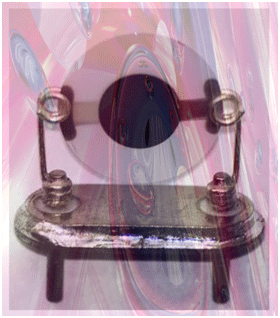
Most crystals, including that shown in Figure 1, vibrate the thickness of a disk. So the thinner the disk is, the higher the frequency at which it will vibrate. To manufacture a crystal with a specific frequency, the thickness must be carefully adjusted to achieve the target frequency. Final calibration is done by etching a small amount of metal (typically silver) away from the electrode. This reduces its mass and forces the frequency rise. The crystal frequency is monitored during the etching – or ion beam tuning – and is stopped when it has reached its target.
Quartz crystal parameters
Many timing ICs use a quartz crystal for the frequency reference Figure 1.
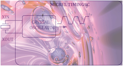
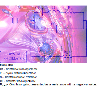
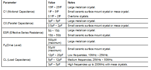
There are certain parameters of a quartz crystal that need to match the parameters of the oscillator circuit for the best frequency accuracy and most reliable operation. The parameters can be best pointed out in the electrical model for the quartz crystal and simplified model for the crystal oscillator, shown in Figure 2.
What do these parameters mean?
C1 and L1
The motional capacitor(C1) represents the elasticity of quartz while the motional inductor(L1) represents the moving mass. As a result, the C1 and L1 circuit is the electrical resonating tank representation of the mechanical resonance in the quartz crystal. The value of C1 is important when trying to tune the frequency of the crystal through changing the load capacitance in the crystal oscillator. The largerthe value of C1, the more frequency deviation from the same load capacitance variation will occur. For example, in a voltage-controlled XTAL oscillator (VCXO) this is important because the VCXO needs to have a specific frequency tuning range. If no frequency tuning is present, the value of C1 is less important. For variations in the load capacitance to have less of an effect on the frequency, a smaller value for C1 may be desirable. The value of L1 is not often specified. Instead, the frequency is specified and we can calculate L1 from C1 and the frequency.
An IC manufacturer may specify C1 in the event it is important to achieve a certain frequency tuning range. Where it is not specified, it is left to the crystal manufacturer to choose the best value based upon manufacturability.
RR, ESR, and RNEG
The resonance resistor (RR) represents the losses in the crystal when it is resonating. The crystal oscillator’s negative resistance will settle at a value that exactly cancels the positive crystal resonance resistance, causing a perpetual oscillation. The values of RNEG and RR in this circuit are not identical because of C0. In typical crystal specifications, a value identified as equivalent series resistance (ESR) is noted. This value is the exact opposite(positive) of the RNEG value in the circuit and can be calculated from the RR, C0, and CL values.
When the crystal oscillator is first turned on, the value of RNEG needs to be much larger than the ESR to grow the oscillation signal quickly. A good rule of thumb is to have the RNEG value equal to at least three times (3X) than ESR value to ensure reliable start-up of the crystal oscillator. When the oscillation amplitude has reached specific amplitude, the nonlinear properties of the oscillator amplifier will prevent the signal from growing further and the RNEG value is effectively reducing to equal ESR value for perpetual oscillation. There are a variety of different methods for setting the oscillation amplitude where the crystal oscillator settles. A manufacturer can provide the value of RNEG in its timing ICs and will specify the ESR or RR to ensure a proper oscillator startup.
C0
C0 is the parallel -or holder -capacitance of the crystal. The electrodes in the crystal typically generate it. At frequencies not near a mechanical resonance of the crystal, the quartz crystal behaves like an ordinary capacitor with a few pico-Farads (pF) of capacitance. The C0 does not have a purpose; it is a parasitic capacitance in the crystal that only has a negative influence on the performance. The IC manufacturer can specify a maximum value so that C0 does not interfere too much with crystal oscillator startup or frequency tuning.
CL
The load capacitance (CL) is a property of the crystal oscillator. Its value influences the exact oscillation frequency of the oscillator with the crystal. To ensure frequency accuracy, crystals are calibrated to resonate at their nominal frequency with a specific load capacitance value. The IC manufacturer can specify the CL value of the crystal oscillator circuit in its timing IC to ensure the proper crystal can be selected. Theoretically, a crystal manufacturer can make any CL value although the most popular values are readily available with most distributers. It is possible to adjust a CL value with an additional capacitor in order to use a popular CL value crystal. With programmable clock generators, CL is programmable and can be customized to a specific crystal in combination with PCB trace capacitance.
FL
FL represents the load frequency where the crystal oscillator will oscillate. In relation to the crystal, it is the oscillation frequency specified at a certain value for the CL. The nominal frequency specified for a crystal will be this load frequency.
FS
The series resonance frequency (FS) of the crystal is determined by C1 and L1. FL is the frequency where the impedance of the crystal is the lowest and, therefore, easy to find with a network analyzer. Some oscillators can oscillate at this frequency, although it is not typical.
Additional considerations
Parameter Interactions and Dependencies
The “perfect” crystal has a low RR or ESR, a low C0 value, and a large C1 value in the event there is a need to tune the frequency. Unfortunately, this “perfect” crystal does not exist due to dependencies between the parameters. Increasing the size of the electrode effectively increases the value of C1 and decreases the value of RR or ESR while also increasing the value of C0. Obviously, the size of the electrode is also limited by the total size of the quartz disc. The smallest SMD crystals are not well suited for use in VCXOs due to the fact that their C1 values cannot be made large enough for adequate frequency tuning. By using larger crystals, a design can be accomplished that provides for a larger electrode for VCXOs and a smaller electrode for non-tuning oscillators. With the smallest SMD crystals, the best that can be accomplished is optimization for a low RR value.
There is a relatively constant ratio between C0 and C1, depending upon how efficiently the electrodes are driving the piezo properties of the quartz. The lower the C0/C1 ratio, the more efficiently the piezo properties are used. Large metal crystals usually have the best efficiency with a C0/C1 ratio close to 200. Small ceramic surface mount crystals perform more poorly with a C0/C1 ratio around 400.
Overtones
A singular quartz crystal can vibrate at a variety of different harmonics. The most common vibration is the “fundamental mode.” This mode is the 1st harmonic and the lowest resonance frequency. Overtones appear at odd multiples of the fundamental mode frequency. For example, there is a 3rd overtone, a 5th overtone, etc. Each overtone can be represented with an extra C1-L1-RRbranch in the crystal model. Generally, the higher the overtone, the higher the RRwill be for that overtone. This is most accurate at the lowest (3rd and 5th) overtones. Typically, a crystal oscillator has more oscillator gain (bigger negative resistance) at lower frequencies and with the RR values at overtones being bigger, without any additional filtering the crystal oscillator will always oscillate at the fundamental mode frequency. The simplest method to make the oscillator oscillate at the 3rd overtone is a high-pass filter to suppress the oscillator gain near the fundamental frequency. If there is sufficient oscillator gain at the 3rd overtone frequency to overcome the RR at the 3rd overtone, the oscillator will oscillate at the 3rd overtone frequency. To oscillate at 5th or higher overtones it is recommended to work with a band-pass filter to suppress both higher and lower tones.
The crystal resonance frequency is a function of the quartz plate thickness. To increase the frequency, the quartz plate thickness needs to be reduced. Thinner crystals can be more difficult to handle during the manufacturing process. Using the crystal at an overtone is a compromise that makes the crystal itself less expensive while making the oscillator circuit more complex.
The vibrating mass is the same at an overtone, making the L1 values of the overtones and the fundamental mode approximately the same. That makes the C1 values much smaller, making the frequency higher (theoretically, 9X smaller for the 3rd overtone, 25X smaller for the 5th overtone, etc.). This sort of overtone operation is not suited for VCXO designs.
Inverted Mesa Technology
The inverted mesa technology makes the crystal very thin in the middle portion of the crystal plate. The thicker outer edges allow for easy handling and the thinner center emits a high fundamental mode frequency when the electrodes are placed only inside the thin area.
The inverted mesa technology is relatively expensive, but for some applications it is worth it (VCXO designs at high frequencies, for example).
Drive Level
The power dissipated in the crystal is the drive level. Above a certain drive level, crystals can show nonlinear properties that can cause unwanted side effects. Coupling with an unwanted vibration mode can occur, resulting in certain frequency instabilities. An IC manufacturer can specify the drive level coming from the crystal oscillator in the timing IC so that a properly functioning crystal can be selected.
Q-Factor
Compared to discretely built tank circuits with LS and CS, the quartz crystal has a very large Q-factor. This parameter is usually not specified, but often expected, of the quartz crystal. The high Q-factor makes the frequency very stable, but another consequence of the high Q-factor is very low noise in the oscillator signal. The Q-factor of a quartz crystal can easily be above 10,000 and sometimes even above 100,000.
A look at crystal frequency accuracy and stability
The resonance frequency of a quartz crystal is very stable compared to alternative techniques such as an LC tank or other materials like ceramic resonators. When used properly, a quartz crystal is a very accurate frequency reference for its cost, which is why quartz crystals are so popular. The frequency accuracy and stability can be broken down into several items:
- Calibration Tolerance at Room Temperature: This is the accuracy of the frequency at nominal conditions. For purposes of identification, “easy” is ±50ppm, “medium” is ±25ppm, and “difficult” is ±10ppm.
- Temperature Drift: Referenced to the frequency at nominal conditions, the frequency drifts with a particular temperature curve. The temperature curve can be modeled with a 3rd order equation and the crystal is usually designed to minimize the drift for a particular temperature range. Selecting a crystal that is specified for the same temperature range as that to which the crystal oscillator circuit will be exposed is advised. The two most common temperature ranges are industrial (-40°C to +85°C) and the commercial (0°C to +70°C). The wider industrial temperature range results in bigger drift numbers or can be more difficult to achieve certain drift requirements with. A <±20ppm drift for the industrial range is considered “difficult”, but it is relatively easy to achieve the same numbers using the commercial range. For the commercial range, a <±10ppmdrift is considered “difficult”.
- Aging: The frequency of a quartz crystal slowly drifts with time due to aging. Mechanical stresses relax over time or small traces of oxygen or moisture can react with the electrode and make the crystal heavier. Usually the direction of the frequency drift with aging is down. The crystal will age quickly in the first few years of use, slowing over time. Occasionally, a manufacturer will pre-age crystals at the factory to meet a very tight aging specification. A typical aging specification is 5ppm per year. Sometimes a specification will read as 5ppm for the first year and lower subsequently.
- Total Stability: This number includes all of the above and this is actually the most popular method for specifying the frequency accuracy of a quartz crystal. It guarantees that the crystal oscillator frequency does not drift outside a certain range under all conditions and for the life of the device. Total frequency numbers like ±100ppm are relatively easy, even with -40°C to +85°C temperature range. Medium is ±50ppm and below that it quickly gets very difficult. Dealing with a total stability requirement, the crystal manufacturer can optimize the frequency accuracy for each individual item for the best manufacturability.
The timing IC itself does not contribute significantly to the accuracy and stability of its output clocks. The accuracy comes from the quartz crystal reference.
The mathematics of crystal oscillators
This formula provides the relation between the ESR value and RR value:
ESR = RR × (1 + C0/CL)2
Where:
- RR = 15W
- C0=3pF
- CL=12pF à ESR = 15 × (1 + 3/12)2 = 23W
The following formula helps calculate frequency movements:
FL = FS × SQRT(1 + C1 / (C0+CL))
The above formula can be used to find the frequency change as a result of a load capacitance change. If CL1 causes FL1 and CL2 causes FL2:
FL1/FL2 = SQRT( (1+C1/(C0+CL1)) / (1+C1/(C0+CL2)) )
Simplified: FL1/FL2 = 1 + 2×C1×(CL2-CL1) / (C0+CL1) / (C0+CL2). When CL1 and CL2 are close together:
dFL = 2000×C1×dCL / (C0+CL)2
dFL is the frequency shift, in ppm (parts per million) caused by the load capacitance shift dCL.C1 is the motional capacitance in fF (fem to farad), dCL is the load capacitance shift in pF (pico farad), C0 is the parallel capacitance in pF, and CL is the nominal load capacitance in pF.
CL Error Example
A crystal is calibrated for CL=12pF and the IC spec also says CL=12pF but there is an additional 1pF parasitic capacitance in the PCB. How large is the frequency error because of the extra 1pF?Additional information for the crystal: C1=8fF and C0=2.5pF.The frequency error dFL = 2000 × 8 × 1 / (2.5 + 12)2 = 76ppm.
VCXO Example
The VCXO specification states:
CL1=20pF at VCONTROL=0V, CL2=8pF at VCONTROL=1.65V and CL3=4pF at VCONTROL=3.3V.
The crystal is calibrated for CL=8pF so the nominal frequency is achieved at VCONTROL=1.65V.The crystal’s parameters are:
C1=8fF(=0.008pF) and C0=2.5pF
With the control voltage tuning between 0V and 3.3V, the frequency tuning range can be calculated by:
FL1/FL2 = SQRT( (1+0.008/(2.5+20)) / (1+0.008/(2.5+8)) ) = 0.999797 = 1 – 203 ppm
FL3/FL2 = SQRT( (1+0.008/(2.5+4)) / (1+0.008/(2.5+8)) ) = 1.000234 = 1 + 234 ppm
The frequency tuning range is -203/+234ppm with 0ppm in the center at VCONTROL = 1.65V.
Fine tuning the load capacitance
When the load capacitance of the timing IC is different from the load capacitance the crystal was calibrated to, the crystal oscillator will not oscillate at the intended nominal frequency of the crystal. We can fix that by adding capacitors to the crystal oscillator circuit. For example, adding a capacitor in series with the crystal lowers the load capacitance of the oscillator circuit (Figure 3).
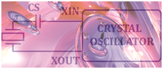
In the event the crystal oscillator load capacitance (CLO) is larger than the load capacitance the crystal is calibrated to (CLX), CS can be added in series to lower the crystal oscillator load capacitance to match the crystal:
CS = CLO×CLX / (CLO – CLX)
Where:
- CLO= 14.32pF
- CLX=12pF à CS = 14.32×12 / (14.32 – 12) = 74pF
When the error is only 2pF or 3pF, a capacitor can be added from XIN to ground to increase the oscillator load capacitance. The problem with this method is that the oscillator gain reduces when adding a capacitor to ground. A more balanced approach is to add a capacitor to ground at both XIN and XOUT (Figure 4).
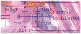
The math is not so precise for this case due to there being various ratios for CLO1/CLO2, so you may need to contact the manufacturer to find out how much capacitance can be added safely in this fashion to a specific timing IC.However, in most cases we can assume the values for CLO1 and CLO2 are quite close to oneanother. To correct the load capacitance 1pF up with CP1 only, CP1=4pF (approximately) must be added. To correct the load capacitance 1pF up with CP1 and CP2, CP1=CP2=2pF (approximately) must be added. Using both CP1 and CP2 is the better method that affects the oscillator gain less.
What about using a reference clock signal instead of a crystal?
Most crystal oscillators allow the XIN pin to be driven with a reference clock signal instead of using a crystal. Although this method is acceptable, there are a few items to consider before implementing it:
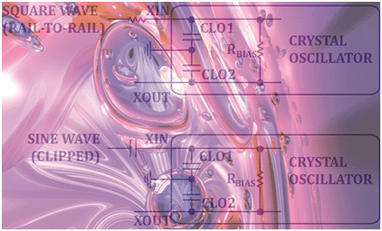
- The usual signal at XIN is a sine wave with a peak-to-peak signal swing smaller than VDD. When applying a square wave to XIN, higher frequency harmonics will couple through CLO1 (Figure 5) to the ground rail and can interfere with other parts of the circuit. When issues such as deterministic jitter or spurs in the phase noise arise, try and slow down the edges on the reference clock square wave with another series resistor. A value of 100Ωis a good first try.
- Most crystal oscillators have DC biasing inside the IC. When using a large signal reference clock with rail-to-rail signal swing, the XIN pin can be directly driven. Conversely, when the reference clock has a smaller signal swing -a TCXO clipped sine wave, for example -it is advised to use a series coupling capacitor to allow the DC biasing to settle at the intended level.
