By Thomas Vetter, ARADEX AG, Germany and Dr. Martin Schulz, Infineon Technologies AG, Germany
During the development of an inverter, control- and power section have to interact smoothly. Highest performance can be achieved by combining smart software with cutting-edge semiconductors and innovative thermal management in a well planned mechanical setup.
Mobile inverter as a decathlete
The basis for an athlete’s success lies within an optimized use and interplay of brain and muscles. Combining both, mental and physical abilities in perfect manner also is the challenge when building an inverter for mobile applications.
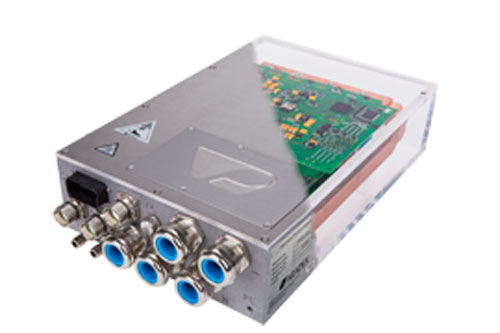
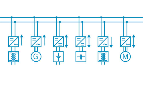
This is especially true if additional functionalities besides driving motors and generators have to be considered. For mobile applications or decentralized drives, the VECTOPOWER concept as displayed in figure 1, can handle a multitude of requirements like
- connection to the grid,
- AC/DC-converter, optionally bidirectional,
- bidirectional connection to batteriesand/or capacitors
- creation of on-board supply or isolated networks.
Figure 2 summarizes the possible scenarios a VECTOPOWER could be used in.
Looking at economical issues, logistics and especially worldwide provision of spare parts, a progressive concept is required. The key is to provide a common hardware for any possible task and make use of proper software or parameters to achieve any functionality desired. This target can be met without compromises if a few major aspects are considered closely.
FPGA as a control center
Having the same topology with six IGBTs installed to support a variety of applications that spans from motor control to DC/DC-converters makes an FPGA a tempting solution for control. A special benefit arises, if the FPGA generates the pulse pattern for the transistors and also administers the high-speed control loops, especially the current control.
The FPGA in the present application observes three voltage- and three current measurements, runs the control algorithms and generates the gate signals for the transistors. The cycle time is reduced down to 2µs. Flexible firmware is the door opener to enable the support of all the tasks hinted at in figure 2.
High speed in functionality and protection
A wide spectrum of functional features combined with a swift and sensitive control is one thing. The other thing, especially in mobile applications, is the extraordinary demand towards protection. Additionally, a wide temperature range and massive mechanical stress, a high demand regarding thermal cycling and varying electric load have to be taken into account, not to mention the stipulation towards save operation under fluctuating system voltage.
Maximizing semiconductor utilization
During short circuit or similarly high overload conditions a proper reaction has to take place within µs. Thermal development inside the semiconductor as a consequence of varying the load usually have to be accounted for in the regime of milliseconds. Detailed, most accurate knowledge of the semiconductor in use is mandatory. Sophisticated methods and model based calculations are done in hard real time inside the FPGA. Depending on the application and the point of operation, this allows an increase in output power by up to 20% from the same semiconductor. This is beneficial for the application both in economics as well as in size and weight especially if advanced protection from extreme operation conditions is achievedat the same time.
A prerequisite to fulfill the sum of requirements is a current control loop that is deterministic, predictable and fast enough to prevent transient overshoots in the load current even at extreme changes.
This particular requirement cannot be matched with common processors. The solution presented therefore is based on FPGA, running several processes in parallel using highly robust state machines.
Utilizing time constants to increase peak power
Especially drive trains demand high peak power for a matter of seconds. Changing the switching frequency on the fly even during active torque control allow to achieve higher peak power. The use of smaller IGBTs is a resulting alternative as well, leading to cost reduction. Choosing a proper switching frequency has to be considered an optimization, taking different parameters into account. Higher switching frequencies lead to decreased losses in the motor due to a reduction of ripple currents. At the same time, it leads to increased switching losses in the power semiconductors.
Comparing the thermal relationsit can be calculated, that a change from 9kHz down to 4.5kHz leads to an increase in output power by 40-45%.
The FPGA-based control allows changing the switching frequency on the fly without introducing distortions to the torque. During normal operation, the frequency remains at 9kHz but may be changed to 4.5kHz for certain points of operation.
The thermal time constants of power semiconductors typically are in a range below 100ms while those for electric motors exceed 100s.
During times of high acceleration or to manage a difficult driveaway situation, this correlation can be considered and the switching frequency can be reduced for a few seconds.
Reducing the amount of magnets in PM-machines
FPGA based control strategies enable a more cost efficient design of power electronics. Further possibilities arise in optimizing permanent motors. The magnets included are very sensitive towards magnetic overload. A few µs of overload are good enough to initiate an irreversible partial demagnetizing. This is why motor designers built in a corresponding magnetic reserve. If, like done with the FPGA, the current can be closely controlled even in a µs scale a motor can be designed featuring the same size, torque, power and efficiency with 30% less magnetic material being used.
The strategic dependency on the raw materials along with the high prices for magnets illustrates, that savings in this dimension are economically essential.
Core piece semiconductor
The power semiconductor is the core component to control the flow of energy. To live up to the expectations, electrical, mechanical and thermal challenges have to be mastered. During the development of an inverter, the semiconductor, the heat sink and the application’s typical load profile have to be considered an inseparable unit. In-depth knowledge about this unit is mandatory to estimate the chip temperature and the temperature swing most accurately. Usually, semiconductor manufacturers provide the information needed by the power system designers to predict the load cycles a semiconductor will survive according to the temperature swing within the application. Knowing the load profiles and the number of cycles to be expected per time, an operating lifetime can be estimated.
For an all electric bus used in public transportation, 60.000 operating hours are demanded during a service life of 15 years representing 1 million kilometers.
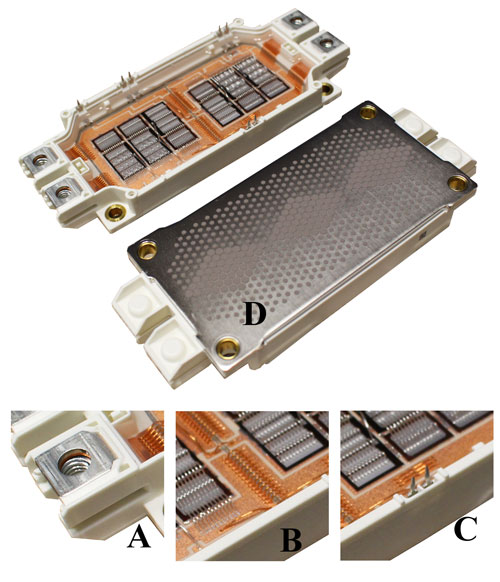
To comply with this demand, EconoDUAL™3 modules were chosen. Exhaustive upgrades have been introduced to the existing design, improving the mechanical robustness, the electric properties and the thermal connection. Figure 3 can best be used to take a look at the changes in detail and their influence to the design.
Interconnecting technologies
Formerly, the power terminals were plugged into the plastic frame. The new design now features injection molded terminals (A) which improves the resistivity towards vibration. Previously, mikromovements of the terminals in some cases induced additional mechanical stress to the bondwires connecting the terminal to the DCB.
A change that improves thermal properties along with electrical capabilities is the new system bonding. System bonds are all wires that interconnect the module’s substrate to each other or provide electrical connection between DCB and terminals. In (B), a detailed view on a part of the new system bonding is given. Instead of using aluminum wires, the connection now is done utilizing copper. The higher specific conductivity enables the handling of higher currents without increasing the number of wires and the space consumed. As a consequence of the lower resistance, the temperature rise in the bond wires is reduced as well. Thus, the material helps to stay within the temperature limits given for the module’s construction even at higher currents.
A further improvement results from replacing solder joints by PressFIT-technology. In demanding applications, solder joints degrade over time due to temperature swing and mechanical wear caused by vibrations. The continuous deterioration eventually leads to so-called cold solder spots. These spots bare the risk of intermittent or lost contact.
The PressFIT technology recently introduced (C) forms a connection to the PCB that is considered a cold welding joint. This is a gas tight, low resistive and mechanically highly robust interconnection. Compared to typical solder- or spring-force contacts, PressFIT-pins improve the connection’s reliability by a factor 100.
Thermal Connection
Improvement regarding the thermal interconnection was achieved by applying a dedicated thermal interface material (TIM) to the power modules. This layer (D) forms the thermal link between power module and heat sink. The new material composition consists of a phase changing carrier matrix that holds the thermally active filler components. The process of application became part of the manufacturing and is fully automated and monitored using a highly sophisticated optical inspection system. This sumptuous procedure ensures that the predefined amount of material is applied in the correct location. The pattern displayed in the picture correlates to the macroscopic geometry of the base plate. Changing the size of the honeycomb varies the amount of material applied locally. The enlarged area that is not covered with TIM later allows direct metal-to-metal contact, leading to further thermal improvement.
Copious tests, substantiated by years of field testing have proven the thermal quality and the long-term stability of the new compound. The critical failure mechanism Pump Out of Thermal Grease now is eliminated.
Enhanced System Soldering
One major novelty especially for modules to support the application Commercial and Agricultural Vehicles (CAV) is the high reliability system solder process. The system solder joint forms the connection between carrier substrate (DCB) and the module’s base plate. Minute deviations between the thermal coefficients of expansion lead to thermal-mechanical stress inside this joint. Delaminating of the layer is a consequence.
This delaminating poses a perturbation of the thermal transfer path as the available area to conduct the heat is reduced. A positive feedback is introduced, as higher chip temperatures result from the diminishing area, leading to a higher temperature swing and increased mechanical stress in turn.
Figure 4 illustrates the evaluation of a system solder joint based on ultrasonic imaging. The images were part of the monitoring during cyclic testing. For comparison, a common solder joint of an industrial-grade device is depicted as well.
For IHM-type modules in the industry sector, the target to be achieved is 3000 cycles. With the newly introduced process for the EconoDUAL™ 3, more than 35.000 cycles have been done under the same conditions, exceeding the target set by factor 10.
More than the sum of its parts
During the development of an inverter, expertise from numerous different disciplines comes together. Only if measurement- and control techniques, software programming, mechanical issues, component selection and thermal management are considered an inseparable unit, outstanding devices with extraordinary capabilities come to existence.
Additional information if needed:
Mobile applications tend to be extreme regarding quality and durability, especially when it comes to vibration. The ARADEX’ VECTOPOWER®, equipped with Infineon’s half bridge modules, survived continuous shock tests acc. to IEC EN60068-2-27 with accelerations of 40g. This is a fundament to support the application CAV with reliable and long-lasting power electronicequipment.


