Bottom termination components (BTCs) are everywhere. It is estimated that nearly 50 billion quad-flat pack no-leads (QFNs), the most common type being BTCs, are used in electronics each year.
Courtesy: Indium Corporation
Industry trends show that number will only increase, given the rising prevalence of “smart” technology. BTCs are no longer restricted to just phones, tablets, and laptop computers. Part of the Internet of Things (IoT), your new car is a veritable computer on wheels, containing numerous computers that let it stream music from your smart phone, connect to the internet, and receive GPS data from orbiting satellites. And don’t forget “smart” home devices, which allow you to check email from your refrigerator, weather from a digital butler, and peek at door-to-door salespeople via doorbells offering facial recognition.
It’s evident there has been, and continues to be, quick growth in electronics and software platforms designed for automobiles, as well as other aspects of the IoT. As technology advances, higher electronic processor speeds produce higher temperatures in electronic components. For automotive electronics, in particular, the higher temperatures pose a cause for concern when considering the high thermal load and harsh conditions that exist, especially under a vehicle’s hood.
Now, more than ever, there is heightened concern for minimizing voiding between the thermal pad and the BTC. It is not uncommon for more than 40% of the thermal pad area to experience solder voiding after reflow, increasing the risk of over-heating of the BTC in field operation.
With our technology and society so dependent on BTCs, it’s important they perform well. So, how do we prevent voiding—one of the electronics assembly’s longest and more troublesome challenges—thus ensuring these critical components remain operationally reliable?
There are two distinct areas of focus: materials and process.
Many have turned to optimized solder paste formulas and vacuum reflow ovens to help reduce voiding. While vacuum reflow ovens all but eliminate voiding, they can cause solder splatter or splash if used improperly. And, solder paste is not a commodity— there are formulas developed to combat specific industry challenges, and some solder paste formulas are simply more effective than others at reducing voids.
Void Origin and Impact
Voids form due to the evaporation of flux materials in the solder paste. With about 50% of solder paste volume consisting of flux, the occurrence of voiding during reflow can be considerable.
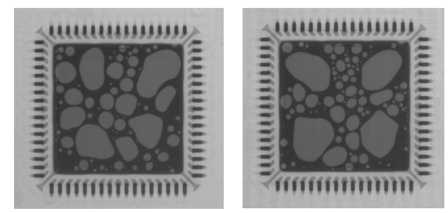
There is no industry standard that sets the bar on how much voiding is acceptable, though there appears to be agreement that a total void area of less than 50%, with no “lake void” greater than 40% of the area, is an absolute requirement (Figure 1). With that said, voiding in smaller amounts, around 25%, is preferred. In some critical applications such as automotive, medical, or defense, 10% or less is required.
Significant voiding can lead to shortened product life. For instance, when an integrated circuit is mounted in a BTC. If assembled with significant voiding, the heat generated by the integrated circuit cannot be dissipated effectively. This excess heat, caused because the air in the void is a very poor conductor of heat, can cause the component to fail. While the total void area on the BTC affects the total amount of heat transmitted, it can be worse to have all the void area in one spot—such as in the previously mentioned lake voids—as it can create a hot spot in the component.
Process: Vacuum Reflow Ovens in SMT Soldering
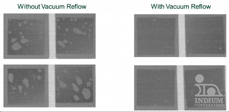
Engineers have made considerable headway in identifying process changes to combat voiding. Reflow oven technology has been adapted to minimize voiding through the use of vacuum reflow to aid in removing voids. Reports suggest that these ovens have been successful in reducing voiding to less than a few percent (Figure 2). While this achievement is significant, it can also require significant investment by the assembler to purchase a new oven, or, at the very least, upgrade machines. While there have also been reports of solder paste spattering, process optimization procedures can minimize this problem.
Some critical recommendations to successfully reduce both voids and solder splatter include:
- Reduce pressure in the oven to about 200mbar (1 atmosphere is 1,000mbar). The steeper the slope, in going from 1,000 to 200 mbar, the more likely you are to produce splattering. Thus, minimizing the slope will help reduce solder splatter.
- The vacuum should be pulled about 30 seconds after the solder becomes molten. This parameter is important, as some fluxes need more time while others less. The time delay before the vacuum is pulled maximizes the chances of solvent volatilization in the flux and prevents solder splatter.
- When possible, keep the vacuum on until after the solder has solidified. Some ovens only have a vacuum chamber in the peak zone; in this case, the vacuum should be kept on as long as possible.
In some cases, what people have thought was solder splatter was actually caused by the stencil printing process. If the stencil under-wipe process or the board gasketing to the stencil is not adequate, solder can be transmitted to the board in areas not originally intended. After reflow, this offending solder can look like solder splatter. To avoid the defect, assure effective under-stencil cleaning and adequate board gasketing is practiced.
Materials: Void-Reducing Solder Paste Formulas
When it comes to voiding, the biggest difference between solder pastes is the flux vehicle. Solder paste is roughly 50% flux vehicle, 50% solder powder by volume, and, typically, 88-90% metal by weight (depending on the alloy and application).
There are a number of flux vehicle options available on the market: no-clean, water-soluble, and rosin mildly activated (RMA). These formulations, all designed to meet different requirements and challenges, vary significantly. Consequently, with regard to voiding, some solder pastes perform better than others.
Solder pastes have been developed to reduce voiding to around 10% without requiring vacuum reflow. Indium Corporation has a suite of materials designed to help Avoid the Void®, including Indium10.1HF and Indium8.9HF solder pastes.
Indium10.1HF Solder Paste is an air reflow, no-clean, halogen-free, Pb-free solder paste specifically formulated to achieve ultra-low voiding, especially in BTC assemblies. It is compatible with lead-free alloys such as SnAgCu, SnAg, and other common alloy systems.
There are factors that have a secondary effect on voiding, such as viscosity, metal load, alloy, and metal mesh size (particle size distribution). Some examples are:
- Higher viscosity materials tend to void more than lower viscosity materials. Imagine air bubbles trying to escape from honey versus air bubbles trying to escape from water. The air bubbles are more likely to be “trapped” by the honey, or viscous materials, versus the water.
- Metal load affects the viscosity of the material and, therefore, affects the BTC voiding performance.
- The wetting energy, or wetting force, of the alloy can have a dramatic effect on voiding performance. The higher the wetting energy the better the resultant BTC voiding results.
Another void-reducing champion is Indium8.9HF Solder Paste—an air reflow, no-clean solder paste specifically formulated to accommodate the higher processing temperatures required by SnAgCu, SnAg, and other alloy systems favored by the electronics industry to replace conventional Pb-bearing solders. It offers unprecedented stencil print transfer efficiency to work in the broadest range of processes. Indium8.9HF utilizes a flux agent system that makes the product stand out, as it has a built-in reoxidation barrier, which has a large impact on void reduction.
Particle size distribution can also have an effect on voiding. As components decrease in size, the solder required to attach them also decreases. The reduced stencil apertures provide smaller deposits and challenge the stencil printing process; however, using finer powder solder pastes have their own challenges. Finer powder solder pastes have more exposed surface area; and, more surface area means more surface oxide, which may increase the amount of voiding.
It is important to consider all aspects and characteristics of a solder paste, as well as the application, simultaneously when determining how to reduce voiding.
The ability to reduce BTC voiding–a long-term industry nuisance–depends on a great number of process variables. Attention to detail through process optimization is just as critical for reduced voiding as the assembly materials. When you are looking to reduce or limit voiding, remember to carefully assess all potential variables in order to determine the root cause of voiding and identify the best solutions to combat it. For more information on reducing voiding, visit www.indium.com/avoidthevoid.


