As design sizes grow, so, too, does the verification effort. Indeed, verification has become the biggest challenge in SoC development, representing a majority share of the development cost, both for hardware itself and for verification at the hardware/software interface. And today, it’s not uncommon for companies to have distributed teams working on multiple SoC designs in parallel. In some cases, teams have been known to share emulation resources amongst tens of projects. In this paper, we’ll discuss the characteristics you should look for to boost your emulation throughput and design team productivity in order to effectively and efficiently manage the delivery and performance targets for multiple, complex SoC designs.
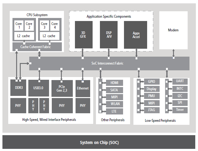
While the average design size in 2014 was about 180 million gates, according to Semico, that size is expected to grow to an average of 340 million gates in 2018. Of course, since these are simply average figures, there are designs that also have more than a billion gates. Large SoCs typically consist of multiple heterogeneous and homogenous integrated processor cores as well as hundreds of clock domains and IP blocks. All of these components need to be verified to ensure that they work as intended. The software executing on the cores adds additional verification challenges and complexity. So while overall design size growth is important, you also need to consider the varied sizes of each of these components. On top of all this, design schedules are as aggressive as ever, given today’s market pressures. See Figure 1 for an example of an advanced SoC.
In reaction to shrinking design cycles, we’re seeing much more hardware design reuse as well as the application of advanced power management techniques, where functions are instead implemented in embedded software.
Design reuse and power management add to the verification challenge, as you need to consider everything from IP interaction at different levels to the interaction between the hardware and software components.
With these considerations, you need a hardware/software verification platform that can simultaneously handle tasks of different sizes and execution lengths, from the smaller IP blocks to sub-systems up to the SoC level. And, you’ll need to extend this verification effort across your enterprise to the other designs that you’re concurrently developing.
The Emulation Throughput Loop
An effective system verification flow integrates a number of techniques:
• Virtual prototyping supports early software development prior to RTL availability, with validation of system hardware/software interfaces as the RTL becomes available and transaction-level models (TLMs) can be run in hybrid configurations with RTL.
• Advanced verification of RTL using simulation is the golden reference today, used in every project. It is focused on hardware verification as it is limited in speed, but unbeatable in bring-up time and advanced debug.
• Simulation acceleration verifies RTL hardware as a combination of software-based simulation and hardware assisted execution, allowing you to reuse your existing simulation verification environment
• Emulation has proven to be effective for hardware/software co-verification with the fastest design bring-up and simulation-like debug, executing jobs of varying sizes and lengths in parallel
• FPGA-based prototyping is applied when RTL matures and provides a pre-silicon platform for early software development, system validation, and throughput regressions
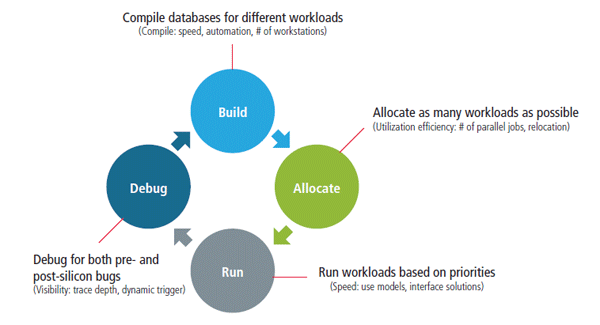
When considering the emulation throughput of a platform and its ROI, it’s important to keep in mind the four major steps in an emulation throughput loop (Figure 2), along with the questions you should ask yourself at each step:
• In the build process, you’re building your verification job, compiling the databases to address different workloads and tasks. Some questions to consider: How fast is the compiler? What is its efficiency and degree of automation for RTL vs. gate-level netlist? How user-friendly is it? How many constructs does it support? Speed in
building these databases is just one parameter, as effective use of resources is also important, particularly since the use model will change as you move through different scenarios in your design.
• Allocation is about allocating the workload as efficiently as possible given a certain resource. Questions to consider here: how many parallel jobs can the system handle? How quickly can you allocate from one resource to another without much user intervention? How do you prioritize and swap these tasks according to demand load? All these significantly impact the workload efficiency with which a compute resource can execute the verification workloads a team has to verify.
• The run step is about execution, but while it may be tempting to focus on how fast the system can run, that’s not the whole story here. This step also pertains to the use model and the interface solutions for that particular use model. Questions to consider: Is the system running jobs based on your design priorities? How many jobs can your system execute in parallel? Can jobs be suspended and resumed? Can a specific point of interest be saved to be resumed from later?
• Debug focuses on detection of pre- and post-silicon bugs. Questions to consider: How well can you debug using the verification platform while minimizing the need to re-run the tests to isolate the bug? How efficiently can you adjust your triggers dynamically without re-compiling? Do you have sufficient debug traces for both HW and SW analysis to allow you to capture a large enough window of debug interest, or do you have to execute multiple times to get the right data to debug?
Each of these steps impacts overall emulation throughput in their own way. For example, debug analysis, considering its data capture and generation requirements, can slow down FPGA-based prototyping and FPGA-based emulation significantly. So you need to decide how much debug is needed for each phase in each particular design. And you might make some adjustments, like using processor-based emulation, during which debug runs un-intrusively at emulation speeds.
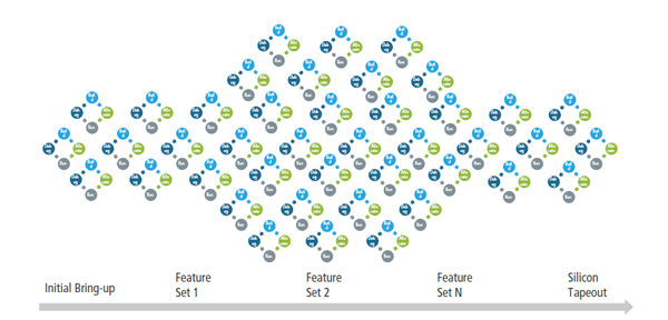
As illustrated in Figure 3, this emulation throughput loop will be repeated multiple times in parallel from initial bring-up to silicon tapeout as you integrate and validate each feature set in your design. So each engineer on your team would go through the process of editing their source, checking, compiling, checking in, and integrating their work with that of their peers. Eventually, and later in the flow, the system becomes deterministic and coherent. Once you’ve settled on your feature set and move into the regression run, you might undergo the emulation loop less often until tapeout.
Why a Holistic View of Parameters for Emulation Throughput Matters
It is also important to take a holistic view of your parameters when you are evaluating emulation throughput.
Consider energy cost—some may calculate this value as intrinsic power over time. However, intrinsic power is merely one portion of the power equation. When comparing, for example, an FPGA-based emulator with a processor-based emulator, you’ll likely find that the total processor-based emulator power can be lower than
in an FPGA-based emulator when you calculate all of the power consumed in a verification task, i.e. adding up compilation (which often needs large parallel server farms for FPGA-based systems), allocation (processor-based emulation may allow better workload efficiency if the granularity of emulation resources is fine enough), execution, and potentially multiple debug runs required to generate comparable amounts of debug information if trace buffers are not appropriately sized.
Also important considerations are job granularity and gate utilization—some systems are simply better designed than others to minimize wasted emulation space and provide faster turnaround times. It’s not only about the number of jobs supported. For example, a system with fine-grained capacity can support more jobs in parallel
while minimizing the resources required. To calculate total turnaround time, you need to consider the number of jobs, the number of parallel jobs that your system can execute, and the run and debug times for this.
How to Support Enterprise-Level Verification Computing Needs?
If you have multiple ongoing design projects involving multiple teams distributed across the globe, not just any verification computing system will do. Enterprise-level verification computing calls for a system that:
• Can scale to billion-gate designs while running within your performance/power targets
• Has the ability to support a high number of daily design turns
• Offers debug productivity with sufficient trace depth to generate the required debug information and fast analysis and compile times
• Can provide the flexibility to allocate a given job to any other domain on the logic board to make the best use of computing resources
• Can offer the efficiency of dynamic resource allocation by breaking up a job in a non-consecutive manner to match the available resource in the system
• Does not lock your jobs to given physical interfaces, instead providing the ability to switch virtually between targets and jobs
Advantages of an End-to-End Flow
Given these parameters, there certainly are advantages to using an end-to-end flow. When an emulation system is part of a set of connected platforms, you can quickly migrate between the interoperable platforms and between hardware/software domains to complete your system-level design, integration, and verification tasks. An integrated flow could provide a substantial boost to design team productivity, while minimizing design risks.
An example of an integrated set of development platforms to support hardware/software design and verification can be found in Cadence’s System Development Suite. The suite’s connected platforms reduce system integration
time by up to 50%, covering early pre-silicon software development, IP design and verification, subsystem and SoC verification, netlist validation, hardware/software integration and validation, and system and silicon validation.
Summary
Clearly, if your design team isn’t using your hardware resources as efficiently or effectively as they could, the team loses valuable productivity. With today’s large, complex SoCs, achieving high levels of multi-user verification throughput and productivity are essential elements of an overall competitive advantage. Many traditional compute resources aren’t equipped to meet these parameters. Instead, today’s designs call for capabilities including high capacity, efficient job allocation, fast runtime, and extensive debug to help you swiftly take your designs to tapeout.
Author:


